

NTE NTE1791 Datasheet
NTE1791
Integrated Circuit
TV Remote Control Amplifier
Description:
The NTE1791 is a silicon monolithic integrated circuit in a 9–Lead SIP type package designed for remote control preamplification of infrared signals. A PIN photo diode can be directly connected to the
input terminal.
This device contains a high gain amplifier, a peak detector, and an output waveform shaper which are
necessary for a remote control preamplifier and has improved light interference–rejection characteristics by use of a two–stage tuning circuit.
The NTE1791 output polarity is active “LOW”.
Features:
D Good Immunity from Light Interference: Narrow Bandwidth ±1.3kHz Typ.
D Operation Voltage: 6V ±10%
D Low Power Consumption: 2.4mA Typ.
D High Input Sensitivity: 50µV
P–P
Typ.
D Peak Detector: The Detector Level is Varied with the Input Signal Level.
D Output Terminal: Open Collector Output. Easy to Interface to Other Devices.
Absolute Maximum Ratings:
Supply Voltage, V
CC
Output Terminal Voltage, V
Power Dissipation, P
D
Operating Temperature range, T
Storage Temperature range, T
(TA = +25°C unless otherwise specified)
OUT
opr
stg
Recommended Operating Conditions:
Parameter Symbol Min Typ Max Unit
Power Supply V
Input Frequency f
CC
in
4.5 5.0 5.5 V
30 – 60 kHz
8V. . . . . . . . . . . . . . . . . . . . . . . . . . . . . . . . . . . . . . . . . . . . . . . . . . . . . . . . . . . . . . . . .
15V. . . . . . . . . . . . . . . . . . . . . . . . . . . . . . . . . . . . . . . . . . . . . . . . . . . . . . .
270mW. . . . . . . . . . . . . . . . . . . . . . . . . . . . . . . . . . . . . . . . . . . . . . . . . . . . . . . . . .
–20° to +75°C. . . . . . . . . . . . . . . . . . . . . . . . . . . . . . . . . . . . . . . . . .
–40° to +125°C. . . . . . . . . . . . . . . . . . . . . . . . . . . . . . . . . . . . . . . . . . .
Electrical Characteristics: (TA = +25°C, VCC = 5V, fin = 40kHz unless otherwise specified)
Parameter Symbol Test Conditions Min Typ Max Unit
Supply Current I
CC
1.6 2.4 3.5 mA
Input Terminal Voltage Vin1 1.0 1.25 1.45 V
Vin2 Iin = 30µA 2.0 2.35 2.5 V
1st Stage Voltage Gain A
Detector Input υ
Input Impedance r
Output Voltage V
Output Leakage Current I
υ
in
OL
OH
L
in
#8 – #4, υ
= 500mV
out
P–P
– 66 – dB
– 50 100 µV
40 60 80 kΩ
IOL = 0.5mA, υin = 1mV
P–P
– – 0.5 V
VOH = 14.4V – – 2 µA
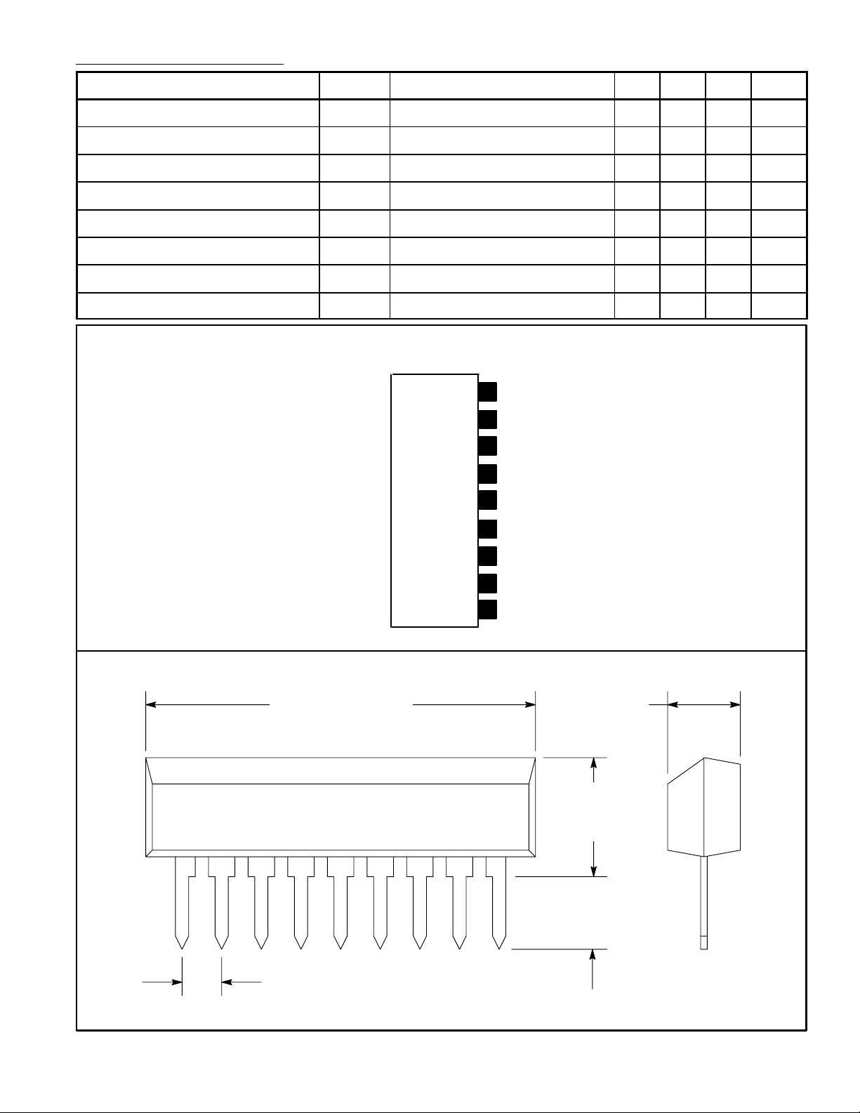
Pin Connection Diagram
(Front View)
V
9
CC
8
Input
7
Peak Hold Detector
Bias Filter
6
5 GND
P–P
st
4
1
Stage Tank
Carrier Filter
3
1
nd
2
2
Stage Tank
1
Output
.900 (22.86)
.110 (2.79)
.226
(5.75)
19
Max
.125
(3.18)
.100 (2.54)
 Loading...