

NTE NTE1789 Datasheet
NTE1789
Integrated Circuit
TV Sound Preamp, AF Output, Volume Control
Description:
The NTE1789 is an integrated circuit in a 9–Lead SIP type package designed for use in TV sound
output circuit.
Features:
D DC Volume Control System
Absolute Maximum Ratings: (TA = +25°C unless otherwise specified)
Supply Voltage, V
Supply Voltage, V
Circuit Voltage, V
Circuit Voltage, V
Circuit Voltage, V
Peak Circuit Current, I
Peak Circuit Current, I
Power Dissipation, P
1–7
9–7
3–7
4–7
6–7
4
8
D
Operating Ambient Temperature Range, T
Storage Temperature Range, T
stg
opr
–10 to +3mA. . . . . . . . . . . . . . . . . . . . . . . . . . . . . . . . . . . . . . . . . . . . . . . . . . . .
–1.2 to +1.2mA. . . . . . . . . . . . . . . . . . . . . . . . . . . . . . . . . . . . . . . . . . . . . . . . . .
–20° to +70°C. . . . . . . . . . . . . . . . . . . . . . . . . . . . . . . . . .
–55° to +150°C. . . . . . . . . . . . . . . . . . . . . . . . . . . . . . . . . . . . . . . . . .
0 to 7V. . . . . . . . . . . . . . . . . . . . . . . . . . . . . . . . . . . . . . . . . . . . . . . . . . . . . . . . . . . . .
0 to V
0 to V
14.4V. . . . . . . . . . . . . . . . . . . . . . . . . . . . . . . . . . . . . . . . . . . . . . . . . . . . . . . . . . . . . .
1.6W. . . . . . . . . . . . . . . . . . . . . . . . . . . . . . . . . . . . . . . . . . . . . . . . . . . . . . . . . . . . .
26V. . . . . . . . . . . . . . . . . . . . . . . . . . . . . . . . . . . . . . . . . . . . . . . . . . . . . . . . . . . . . . . .
1–7
9–7
V. . . . . . . . . . . . . . . . . . . . . . . . . . . . . . . . . . . . . . . . . . . . . . . . . . . . . . . . . .
V. . . . . . . . . . . . . . . . . . . . . . . . . . . . . . . . . . . . . . . . . . . . . . . . . . . . . . . . . .
Electrical Characteristics: (TA = +25°C unless otherwisepsecified)
Parameter Symbol Test Conditions Min Typ Max Unit
Circuit Current I
Circuit Voltage V
V
V
V
Max. Output Voltage POmax V4 = 12V, f = 1kHz, THD = 10% 2.0 2.3 – W
Voltage Gain G
Total Harmonic Distortion THD V4 = 12V, PO = 1W, f = 1kHz – 0.8 1.2 %
Max. Attenuation A
Output Noise Voltage V
Mute Operating Voltage V
SW1: 1, SW2: 1 7.1 9.5 11.9 mA
I
SW1: 2, SW2: 1 – 5.4 – V
2–7
SW1: 2, SW2: 1 – 8.5 – V
5–7
SW1: 2, SW2: 1 – 8.8 – V
6–7
SW1: 2, SW2: 2 – 8.8 – V
8–7
V4 = 12V, Vi = 0.1V
V
f = 1kHz, Vi = 0.1V
tt
V4 = 12V and V4 = 0V
V4 = 0V, Vi = 0V
no
f = 1kHz, V4 = 12V, when V8 = 0V
3–7
, f = 1kHz 28.5 30.5 32.5 dB
rms
, Ratio between
rms
rms
rms
– –95 –85 dB
– 0.6 1.0 mV
2.45 2.65 2.85 V
rms
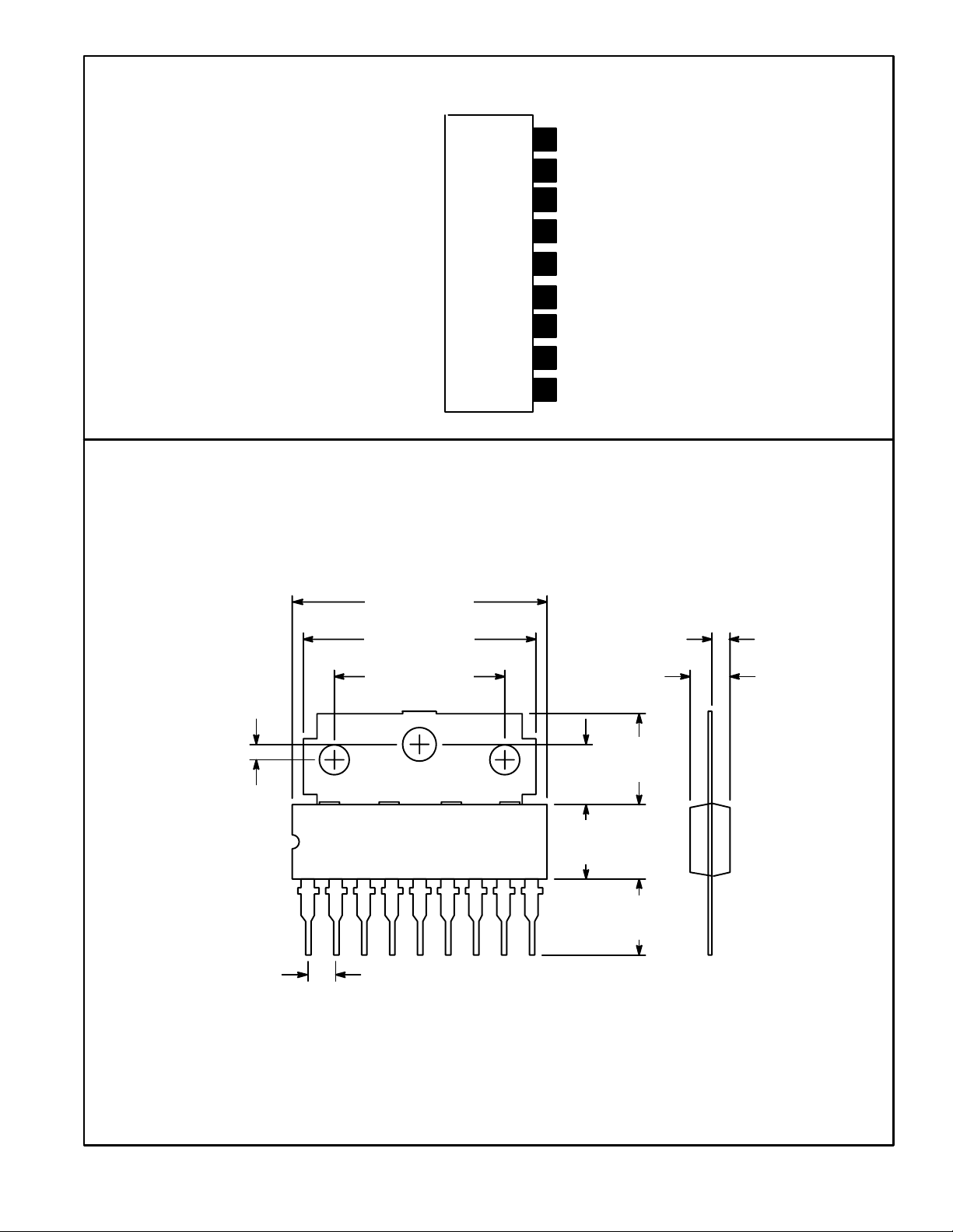
Pin Connection Diagram
(Front View)
9
8
7
6
5
4
3
2
1
VCC 2 (18V Typ)
Sound Output
GND
Feedback
Filter
Volume Control
Mute
Sound Input
VCC 1 (12V Typ)
.059
(1.5)
.890 (22.6)
.728 (18.5)
.591 (15.0)
.067 (1.72)
.150 (3.8)
.328
.229
(8.33)
(5.82)
.250
(6.35)
19
.281
(7.14)
.100 (2.54)
 Loading...