

NTE NTE1786 Datasheet

NTE1786
Integrated Circuit
Frequency Lock Loop (FLL)
Tuning & Control Circuit
Description:
The NTE1786 is an integrated circuit in a 24–Lead DIP type package that provides closed–loop digital
tuning of TV receivers, with or without AFC, as required. This device also controls up to 4 analog functions, 4 general purpose I/O ports and 4 high–current outputs for tuner band selection.
Features:
D Combined Analog and Digital Circuitry Minimizes the Number of Additional Interfacing Components
Required
D Frequency Measurement with Resolution of 50kHz
D Selectable Prescaler Divisor of 64 or 256
D 32V Tuning Voltage Amplifier
D 4 High–Current Outputs for Direct Band Selection
D 4 Static Digital–to–Analog Convertors (DACs) for Control of Analog Functions
D 4 General Purpose Input/Output (I/O) Ports
D Tuning with Control of Speed and Direction
D Tuning with or without AFC
D Single–Pin, 4MHz On–Chip Oscillator
2
D I
C Bus Slave Transceiver
Applications:
D TV Receivers
D Satellite Receivers
D CATV Converters
Absolute Maximum Ratings:
Supply Voltage Ranges,
Pin13, V
Pin19, V
Pin14, V
CC1
CC2
CC3
–0.3 to +18V. . . . . . . . . . . . . . . . . . . . . . . . . . . . . . . . . . . . . . . . . . . . . . . . . . . . . . . . .
–0.3 to +18V. . . . . . . . . . . . . . . . . . . . . . . . . . . . . . . . . . . . . . . . . . . . . . . . . . . . . . . . .
–0.3 to +36V. . . . . . . . . . . . . . . . . . . . . . . . . . . . . . . . . . . . . . . . . . . . . . . . . . . . . . . . .
Absolute Maximum Ratings (Cont’d):
Input/Output Voltage Ranges,
Pin2, V
Pin3, V
Pin4 to Pin7, V
Pin8 & Pin9 (Note 1), V
Pin10, V
Pin12 (Note 2), V
Pin15 to Pin18 (Note 2), V
Pin20 (Note 1), V
Pin21, V
Pin1, Pin22 to Pin24 (Note 1), V
Total Power Dissipation, P
Operating Ambient Temperature Range, T
Storage Temperature Range, T
SDA
SCL
P2X
, V
AFC+
. . . . . . . . . . . . . . . . . . . . . . . . . . . . . . . . . . . . . . . . . . . . . . . . . . . . . . . . . . .
TI
. . . . . . . . . . . . . . . . . . . . . . . . . . . . . . . . . . . . . . . . . . . . . . . . .
TUN
. . . . . . . . . . . . . . . . . . . . . . . . . . . . . . . . . . . . . . . . . . . . . . . . .
FDIV
OSC
TOT
stg
AFC–
. . . . . . . . . . . . . . . . . . . . . . . . . . . . . . . . . . . . . . . . . .
P1X
. . . . . . . . . . . . . . . . . . . . . . . . . . . . . . . . . . . . .
DACX
. . . . . . . . . . . . . . . . . . . . . . . . . . . . . . . . . . .
A
Note 1. Pin voltage may exceed supply voltage if current is limited to 10mA.
Note 2. Pin voltage must not exceed 18v but may exceed V
DC and AC Electrical Characteristics:
(TA = +25°C, V
CC1
of current is limited to 200mA.
CC2
, V
CC2
, V
at typical voltages
CC3
unless otherwise specified)
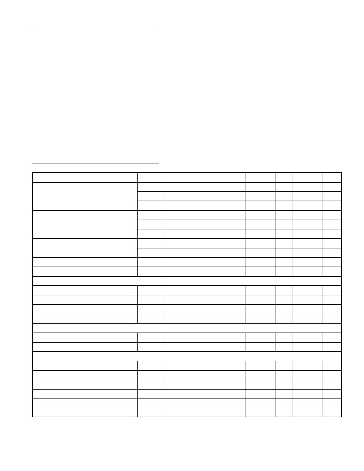
Parameter Symbol Test Conditions Min Typ Max Unit
Supply Voltage V
Supply Current (No Outputs Loaded) I
Additional Supply Currents (A) I
Total Power Dissipation P
Operating Ambient Temperature T
I2C Bus Inuts SDA Input (Pin2); SCL Input (Pin3)
Input Voltage, HIGH V
Input Voltage, LOW V
Input Current, HIGH I
Input Current, LOW I
I2C Bus Outputs SDA Output (Pin2, Open Collector)
Output Voltage, LOW V
Maximum Output Sink Current I
Open–Collector I/O Ports P20, P21, P22, P23 (Pin4 to Pin7, Open Collector)
Input Voltage, HIGH V
Input Voltage, LOW V
Input Current, HIGH I
Input Current, LOW I
Output Voltage, LOW V
Maximum Output Sink Current I
CC1
V
CC2
V
CC3
CC1
I
CC2
I
CC3
CC2A
I
CC3A
TOT
IH
IL
OL
OL
IH
IL
OL
OL
Note 3 –2 – I
Note 3 0.2 – 2.0 mA
A
Note 4 3 – VCC–1 V
IH
IL
Note 4 – – 10 µA
IOL = 3mA – – 0.4 V
IH
IL
IOL = 2mA – – 0.4 V
10.5 12.0 13.5 V
4.7 13.0 16.0 V
30 32 35 V
18 30 45 mA
0 – 0.1 mA
0.2 0.6 2.0 mA
– 380 – mW
–20 – +70 °C
–0.3 – 1.5 V
– – 10 µA
– 5 – mA
2 – 16 V
–0.3 – 0.8 V
– – 25 µA
– – 25 µA
– 4 – mA
–0.3 to +18V. . . . . . . . . . . . . . . . . . . . . . . . . . . . . . . . . . . . . . . . . . . . . . . . . . . . . . . . . .
–0.3 to +18V. . . . . . . . . . . . . . . . . . . . . . . . . . . . . . . . . . . . . . . . . . . . . . . . . . . . . . . . . .
–0.3 to +18V. . . . . . . . . . . . . . . . . . . . . . . . . . . . . . . . . . . . . . . . . . . . . . . . . . . .
–0.3 to V
–0.3 to V
–0.3 to V
–0.3 to V
–0.3 to V
–0.3 to +5V. . . . . . . . . . . . . . . . . . . . . . . . . . . . . . . . . . . . . . . . . . . . . . . . . . . . . . . . . .
–0.3 to V
–20° to +70°C. . . . . . . . . . . . . . . . . . . . . . . . . . . . . . . . . . .
–65° to +150°C. . . . . . . . . . . . . . . . . . . . . . . . . . . . . . . . . . . . . . . . . .
OHP1X
CC1
CC1
CC3
CC2
CC1
CC1
1000mW. . . . . . . . . . . . . . . . . . . . . . . . . . . . . . . . . . . . . . . . . . . . . . . . . . .
mA
Note 3. For each band–select output which is programmed at logic 1, sourcing a current I
additional supply currents (A) shown must be added to I
Note 4. If V
< 1V, the input current is limited to 10µA at input voltages up to 16V.
CC1
CC2
and I
, respectively.
CC3
OOP1X
, the
 Loading...