

NTE1767
Integrated Circuit
Vertical Deflection Output Circuit
for Color TV
Description:
The NTE1767 is a vertical deflection output circuit in a 8–Lead SIP type package for use in Color TV
applications of 22 inch or larger. This device requires no voltage–boosted pulses and, therefore, can
be connected to a chrominance–video deflection circuit (NTE1793), deflection circuit (NTE1664), or
the like.
Features:
D Requires High Power Voltage only during Flyback Time, Greatly Reducing Power Consumption
D Deflection Control in the Preceeding Stage can be used both by Discrete Components and ICs
Absolute Maximum Ratings:
Power Supply Voltage, V
Circuit Current, I
CC
Deflection Circuit Voltage, V
Deflection Input Signal Voltage, V
Deflection Output Current, I
Voltage Booster Output Current, I
Voltage Booster Output Voltage, V
Allowablw Power Dissipation, P
Operating Temperature Range, T
Storage Temperature Range, T
Junction Temperature, T
J
(TA = +25°C, Note 1, unless otherwise specified)
(V6) 30V. . . . . . . . . . . . . . . . . . . . . . . . . . . . . . . . . . . . . . . . . . . . . . . . . . . . . .
DC
3
4
(I2) –1.5 to +1.5A
DEF
. . . . . . . . . . . . . . . . . . . . . . . . . . . . . . . . . . . . . .
. . . . . . . . . . . . . . . . . . . . . . . . . . . . . . . . . . . . . . .
7
7
D
opr
stg
–1.5 to +1.5A
–20° to +75°C. . . . . . . . . . . . . . . . . . . . . . . . . . . . . . . . . . . . . . . . .
–40° to +150°C. . . . . . . . . . . . . . . . . . . . . . . . . . . . . . . . . . . . . . . . . .
Note 1. A positive current flows into the NTE1767 and a negative current flows out of it.
Recommended Operating Conditions:
Parameter Symbol Test Conditions Min Typ Max Unit
Power Supply Voltage (V6) V
Deflection Output Current (I2) I
(TA = +25°C unless otherwise specified)
CC
DEF
20 24 27 V
1.0 – 2.1 A
350mA. . . . . . . . . . . . . . . . . . . . . . . . . . . . . . . . . . . . . . . . . . . . . . . . . . . . . . . . . . . . . .
65V. . . . . . . . . . . . . . . . . . . . . . . . . . . . . . . . . . . . . . . . . . . . . . . . . . . . . . . .
2.5V. . . . . . . . . . . . . . . . . . . . . . . . . . . . . . . . . . . . . . . . . . . . . . . . . .
PEAK
PEAK
V6 V. . . . . . . . . . . . . . . . . . . . . . . . . . . . . . . . . . . . . . . . . . . . . . . . . .
8W. . . . . . . . . . . . . . . . . . . . . . . . . . . . . . . . . . . . . . . . . . . . . . . . . . . . .
+150°C. . . . . . . . . . . . . . . . . . . . . . . . . . . . . . . . . . . . . . . . . . . . . . . . . . . . . . . . .
P–P
Electrical Characteristics: (VCC = 24V, TA = +25°C, RL = 8Ω, 9.4mH unless otherwise specified)
Parameter Symbol Test Conditions Min Typ Max Unit
Power Supply Current I
Deflection Current I
Neutral Point Potential V
OC
DEF
ODC
240 270 300 mA
1.9 2.0 2.1 A
P–P
10 12 14 V
Flyback Pulse Voltage RPV 46 49 54 V
Blanking Pulse Width RPW 550 650 750 µs
Idling Current I
Voltage Booster Discharge Saturation Voltage V
Voltage Booster Charge Saturation Voltage V
S6–7
S7–1
Voltage Booster Charge Current I
Deflection Circuit Output Saturation Voltage V
V
S2–1
S3–2
Deflection Circuit Input Saturation Voltage V
Voltage Gain A
Input Resistance R
Thermal Resistance, Junction–to–Case R
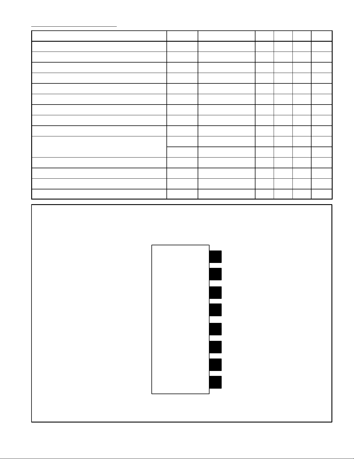
Pin Connection Diagram
(Front View)
VO
Θ
Q
7
4
in
JC
8 16 24 mA
– 1.8 2.4 V
– 1.0 1.5 V
55 85 120 mA
– 1.0 1.6 V
– 2.4 3.0 V
0.85 1.0 1.15 V
– 55 – dB
– 22 – kΩ
– – 4.0 °C/W
8
N.C.
7
Voltage Booster Output
V
6
5
CC
Capacitor for Preventing
Oscillation
Input
4
Power for Vertical
3
2
1
1
Deflection Output
Deflection Output
GND
 Loading...