

NTE NTE1766 Datasheet
NTE1766
Integrated Circuit
Reversible Motor Driver
Description:
The NTE1766 is a reversible motor driver in a 10–Lead SIP type package capable for directly driving
a motor containing a brush, requiring reversible rotation.
Features:
D High Output Current: IOmax = 2.2A
D Built–In Thermal Shutdown Circuit
D Output Voltage Setting Terminal
D Low Circuit Current in Standby Mode
Absolute Maximum Ratings
Supply Voltage, V
Output Current, I
Input Voltage, V
Power Dissipation (T
, V
CC1
2.2A. . . . . . . . . . . . . . . . . . . . . . . . . . . . . . . . . . . . . . . . . . . . . . . . . . . . . . . . . . . . . . . .
O
IN
= +25°C), P
A
: (TA = +25°C unless otherwise specified)
CC2
D
Derate Above 25° 22mW/°C. . . . . . . . . . . . . . . . . . . . . . . . . . . . . . . . . . . . . . . . . . . . . . . . . . . . . . .
Operating Temperature Range, T
Storage Temperature Range, T
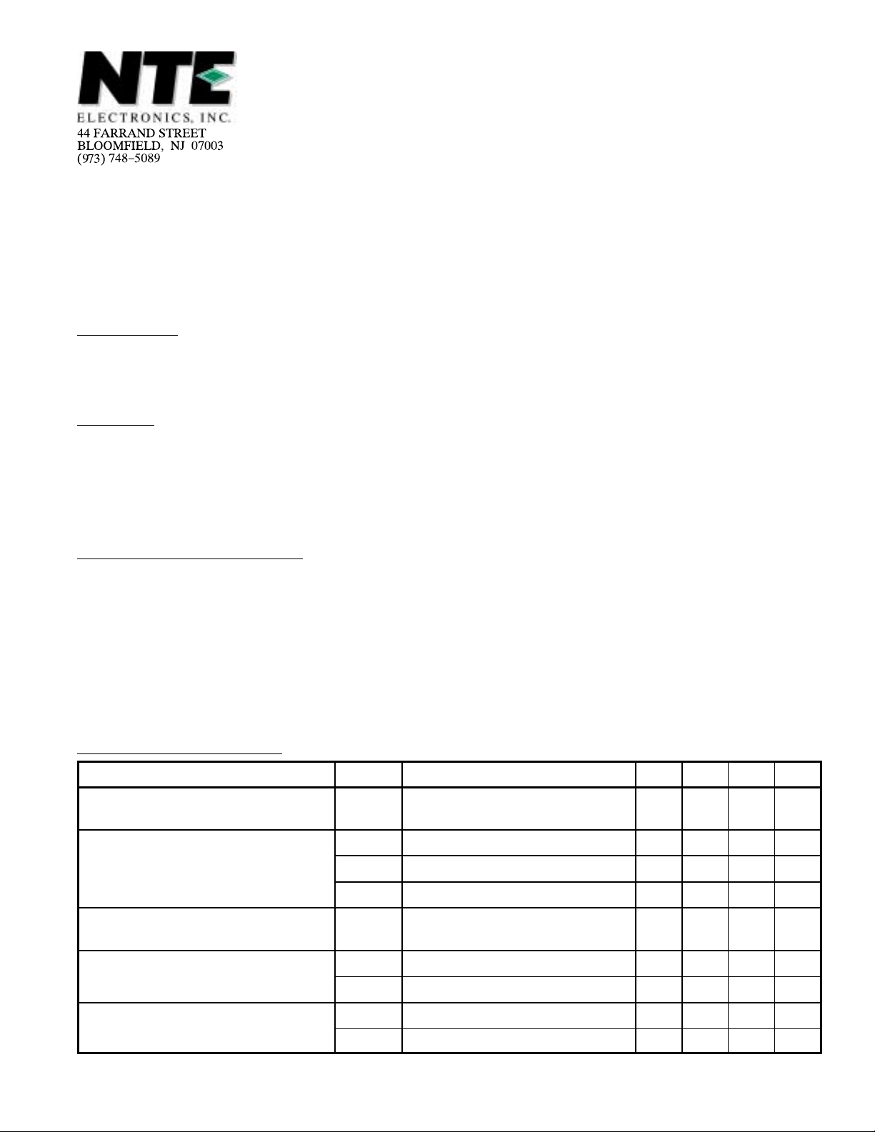
Electrical Characteristics
Parameter Symbol Test Conditions Min Typ Max Unit
Supply Voltage V
Supply Current I
Threshold Voltage, Pin5, Pin6 V
Voltage Level, Pin2 V
Voltage Level, Pin10 V
: (TA = +25°C, VCC = 12V unless otherwise specified)
opr
stg
V
I
I
V
V
V
CC1
CC2
CC1
CC2
CC3
TH5
TH6
H2
L2
H10
L10
–0.3V to V
–20° to +75°C. . . . . . . . . . . . . . . . . . . . . . . . . . . . . . . . . . . . . . . . .
–50° to +125°C. . . . . . . . . . . . . . . . . . . . . . . . . . . . . . . . . . . . . . . . . .
,
Pin5, Pin6, “L” – 1.2 2.5 mA
Pin5, Pin6 – 16 35 mA
Pin5, Pin6, “H” – 25 60 mA
,
“L” Level ≤ 1V, “H” Level ≥ 3V 1.0 2.0 3.0 V
RL = 60Ω, ZD = 6.8V 6.5 – – V
RL = 60Ω – – 1.2 V
RL = 60Ω, ZD = 6.8V 6.5 – – V
RL = 60Ω – – 1.2 V
8 – 18 V
24V. . . . . . . . . . . . . . . . . . . . . . . . . . . . . . . . . . . . . . . . . . . . . . . . . . . . . . . . .
V. . . . . . . . . . . . . . . . . . . . . . . . . . . . . . . . . . . . . . . . . . . . . . . . . . . . . . .
CC1
2200mW. . . . . . . . . . . . . . . . . . . . . . . . . . . . . . . . . . . . . . . . . . . . .
Input/Output Truth Table:
Input Output
Pin5 Pin6 Pin2 Pin10
L L OPEN OPEN
H L H L
L H L H
H H L L
Note 1. Input Level “H”: 3.0V
Input Level “L”: 1.0V
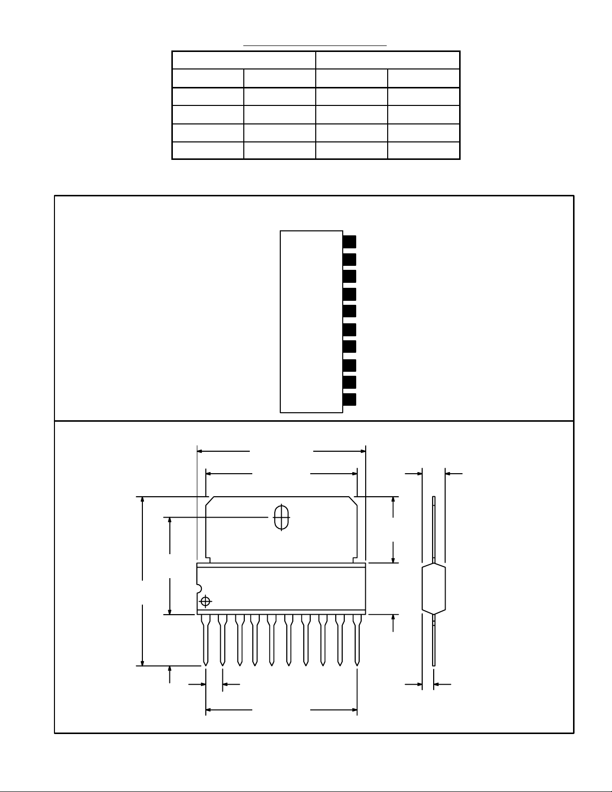
Pin Connection Diagram
(Front View)
10
V
9
V
8
V
7
V
6
5
4
V
3
V
2
V
1
1.043 (26.5)
.984 (25.0)
OUT2
Z2
CC2
CC1
Reverse Input
Forward Input
R
V
Z1
OUT1
GND
.141
(3.6)
1.063
(27.0)
.700
(17.78)
.251
(6.4)
.409
(10.4)
.330
(8.38)
110
.100 (2.54)
.070
(1.78)
.897 (22.8)
 Loading...