

NTE NTE1764 Datasheet
NTE1764
Integrated Circuit
Infrared Preamplifier
Description:
The NTE1764 is an infrared preamplifier in a 14–Lead DIP type package and contains four main parts:
the gain–controlled amplifier I, the amplifier II, the pulse–separating amplifier III, and the inverter IV.
The amplifier I has a wide dynamic range and thus ensures interference free operation, also at bright
ambient light, 50Hz modulated light originating from fluorescent lamps, or at intensive infrared light,
e.g. produced by infrared sound transmission. It is also possible, to approach almost directly the remote–control transmitter to the receiver without producing misfunction by overdriving the receiver.
The amplifier II further amplifies the signal, and amplifier III separates the pulse–shaped intelligence
signal from noise and other unwanted parts. The inverter IV provided additionally inverts the output
signal available at Pin7 as negative pulse, and thus delivers positive output pulses at Pin8. If an additional resistor is inserted between Pin6 and GND, the noise–immunity is increased, but the input sensitivity decreased. Pin10 serves as test pin and must not be connected.
The capacitor connected from Pin2 to GND influences the automatic gain control of amplifier I contained in the NTE1764. A capacitance of less than 1µF will cause misfunction in the distance range
of 0.2, to 2m.
Absolute Maximum Ratings:
Supply Voltage, V
6V. . . . . . . . . . . . . . . . . . . . . . . . . . . . . . . . . . . . . . . . . . . . . . . . . . . . . . . . . . . . . . . . . .
3
Ambient Operating Temperature Range, T
Storage Temperature Range, T
Recommended Operating Conditions:
Supply Voltage V
(Note 1)
–30° to +125°C. . . . . . . . . . . . . . . . . . . . . . . . . . . . . . . . . . . . . . . . . . .
S
Parameter
–20° to +65°C. . . . . . . . . . . . . . . . . . . . . . . . . . . . . . . . . .
A
(Note 1)
Symbol Min Typ Max Unit
3
4.5 5.0 5.5 V
Electrical Characteristics: (V3 = 5V, TA = +25°C, Note 1)
Parameter Symbol Min Typ Max Unit
Current Consumption I
2
– 1 2 mA
Gain Between Pin14 & Pin7 G 70 – – dB
Output Resistance Pin7 & Pin8, formed by the Pull–Up of an
R
O
– 20 – kΩ
NPN Transistor
Output Low Voltage Pin7 & Pin8 at IOL = 1.6mA V
OL
– 0.4 0.8 V
IR Transmission Range using the SAA1250 IR Transmitter IC
and a Transmission Current Amplitude of 1.5A, and
One Transmitter Diode (NTE3017)
L1 – 12 – m
Two Transmitter Diodes (NTE3017) L2 – 19 – m
Three Transmitter Diodes (NTE3017) L3 – 20 – m
Note 1. All voltages are referred to GND (Pin1, Pin9, and Pin13).
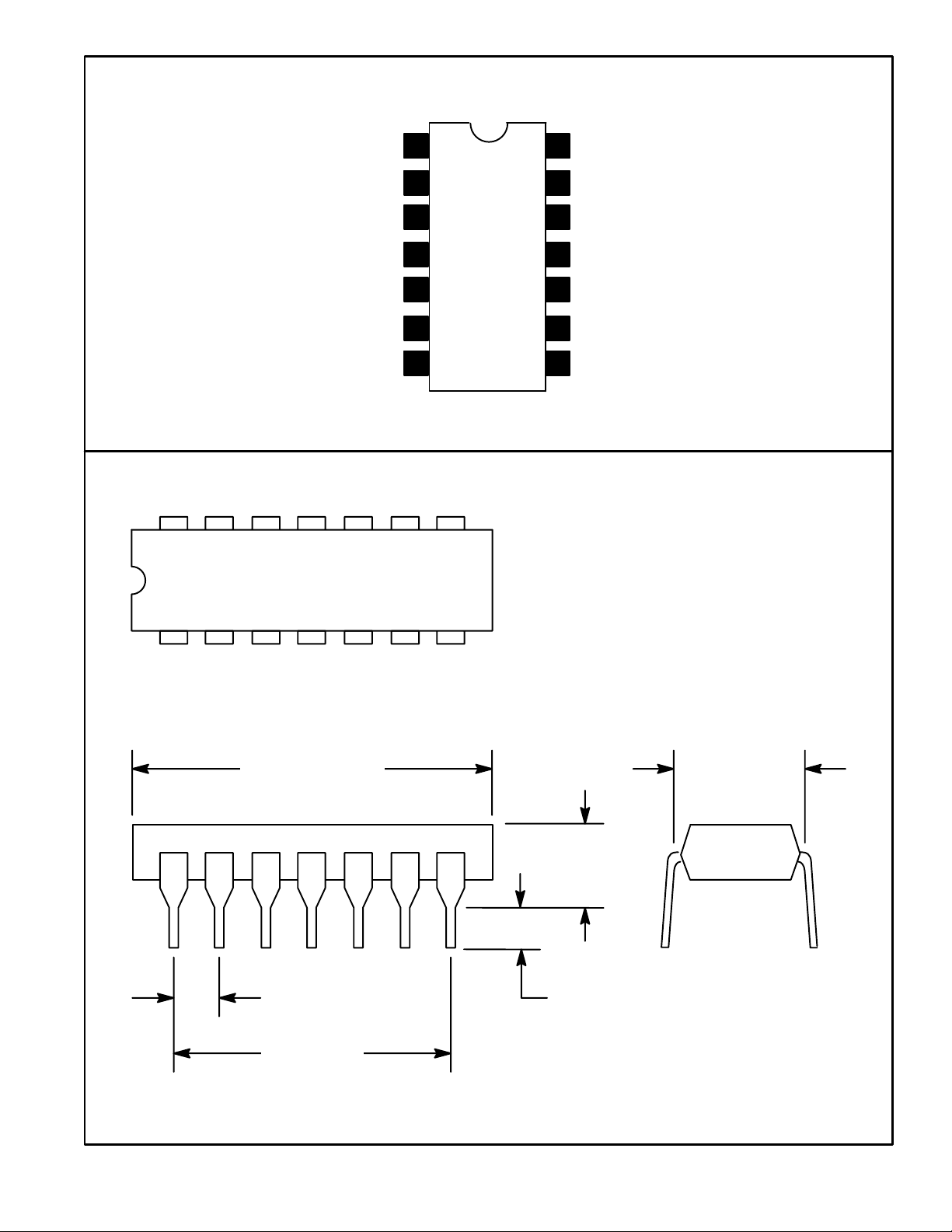
Pin Connection Diagram
Input’s GND, 0
Capacitor Pin Amplifier I
Supply Voltage V
Input Amplifier III
1
2
3
B
4
5Output Amplifier II
6Separation Threshold Adjust
7Negative Pulse Output
14 8
14
Input Amplifier I
13
GND, 0, of Amplifier II
12
Ouptut Amplifier I
11
Input Amplifier II
10 Test Pin/N.C.
9 Output’s GND, 0
8 Positive Pulse Output
17
.785 (19.95) Max
.300 (7.62)
.200
(5.08)
Max
.100 (2.45) .099 (2.5) Min
.600 (15.24)
 Loading...