

NTE NTE1759 Datasheet
NTE1759
Integrated Circuit
PMOS, 26 Command TV Remote Control Reciever
Description:
The NTE1759 is a PMOS integrated circuit in a 16–Lead DIP type package designed for use in decoding the signal received from a transmitter in TV remote control applications. Direct channel selection
can be obtained by combining the NTE1759 receiver with the NTE1758 transmitter control IC. When
using the NTE1520 as the channel selection IC, a complete remote control system can be obtained.
Features:
D Capable of Receiving 26 Commands:
Channel 1–20 Channel UP/DOWN
Volume UP/DOWN Mute ON/OFF
Power ON/OFF
D Capable of Controlling 5 Commands Directly:
Channel UP/DOWN
Volume UP/DOWN
Power ON/OFF
D By Combining with the NTE1520, Direct Addressing is Easily Realized
D Capable of Controlling the Volume for 31 Steps
Absolute Maximum Ratings:
Supply Voltage, VDD –V
Input Voltage, V
Output Current I
IN
OH
–V
SS
SS
(TA = +25°C unless otherwise specified)
–15 to +0.3V. . . . . . . . . . . . . . . . . . . . . . . . . . . . . . . . . . . . . . . . . . . . . . . . . . .
–VDD to +0.3V. . . . . . . . . . . . . . . . . . . . . . . . . . . . . . . . . . . . . . . . . . . . . . . . . . . .
CHU, CHD, INI –5.0mA. . . . . . . . . . . . . . . . . . . . . . . . . . . . . . . . . . . . . . . . . . . . . . . . . . . . . . . . . . .
VOL, POW –10.0mA. . . . . . . . . . . . . . . . . . . . . . . . . . . . . . . . . . . . . . . . . . . . . . . . . . . . . . . . . . . . .
Power Dissipation, P
Operating Temperature Range, T
Storage Temperature Range, T
Electrical Characteristics:
Parameter Symbol Test Conditions Min Typ Max Unit
Supply Voltage V
Supply Current I
Input High Voltage VIH(1 ∼ 5, 13) 0 – –1.5 V
Input Low Voltage VIL(1 ∼ 5, 13) –5.0 – V
Input Pulldown Current IIL(1 ∼ 5, 13) TA = +25°C, VIN = VSS, VDD = –12V 5.0 – 50 µA
D
opr
stg
–20° to +75°C. . . . . . . . . . . . . . . . . . . . . . . . . . . . . . . . . . . . . . . . .
–40° to +125°C. . . . . . . . . . . . . . . . . . . . . . . . . . . . . . . . . . . . . . . . . .
(TA = –20° to +75°C, VDD = –9.6 to +14.4V unless otherwise specified)
DD
DD
TA = +25°C, OSCI = VSS, VDD = –12V –4.0 –10.0 –20.0 mA
–9.6 –12.0 –14.4 V
360mW. . . . . . . . . . . . . . . . . . . . . . . . . . . . . . . . . . . . . . . . . . . . . . . . . . . . . . . . . .
DD
V
Electrical Characteristics (Cont’d): (TA = –20° to +75°C, VDD = –9.6 to +14.4V unless otherwise
specified)
Parameter Symbol Test Conditions Min Typ Max Unit
Output High Voltage VOH(CHU) IOH = –1.0mA – – –2.5 V
Output High Voltage VOH(CHD) IOH = –1.0mA – – –2.5 V
Output High Voltage VOH(INI) IOH = –1.0mA – – –2.5 V
Output High Voltage VOH(VOL) IOH = –5.0mA – – –2.5 V
Output High Voltage VOH(POW) IOH = –5.0mA – – –2.5 V
Output Low Current IOL(1 ∼ 5, 13) TA = +25°C, VOL = –11.5V, VDD = –12V 0 – 100 µA
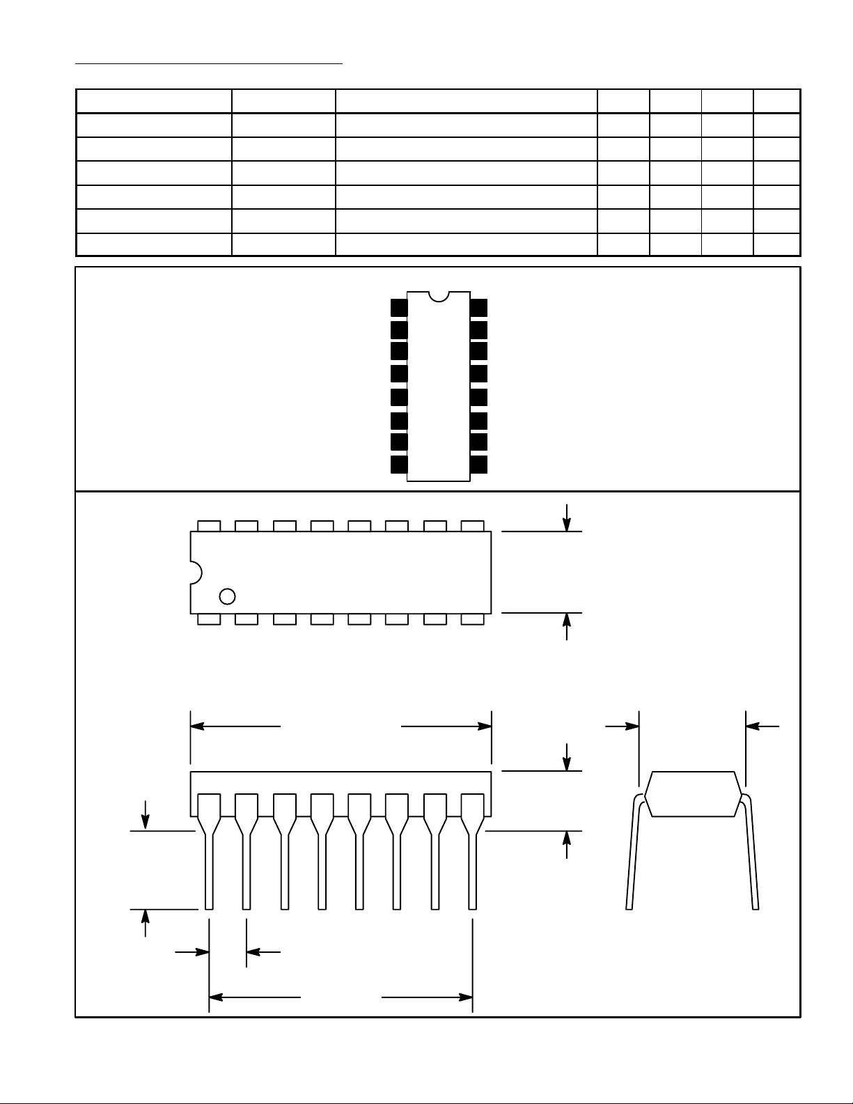
Pin Connection Diagram
POW Input
CHU Input
CHD Input
VOL Up Input
VOL Down Input
POW Output
VOL Output
(GND)
DD
16 9
18
1
2
3
4
5
6
7
D)V
8
16
INI Output (Optional for Free Use)
15
CHD Output
14
CHU Output
13
Remote Signal Input
(–12V)
V
12
SS
11
OSC Output
10
OSC Input
9
Test
.260
(6.6)
Max
.245
(6.22)
Min
.785 (19.9) Max
.100 (2.54)
.700 (17.7)
.300 (7.62)
.200
5.08)
Max
 Loading...