

NTE1757
Integrated Circuit
Remote Control Receiver
Description:
The NTE1757 is an MOS/LSI integrated circuit in an 18–Lead DIP tpye package designed for use
as a receiver of remote control signals generated by a transmitter circuit, using PPM (Pulse Position
Modulation) encoding technique. The receiver has 5 digital outputs whose response to PPM codes
may be programmed by six control lines. It has a handshake interface which provides communication
with microprocessors and computers.
Features;
D 5 Open Drain Outputs with Enable
D Handshake or Interrupt Microprocessor and Computer Interface Signals
D On–Chip Oscillator
D 6 Control Lines to Program Output Response
D 3 Selectable Output Modes
Absolute Maximum Ratings:
VDD Supply and All Inputs wrt, V
Storage Temperature Range, T
SS
stg
Operating Ambient Temperature Range, T
A
+0.3 to –25V. . . . . . . . . . . . . . . . . . . . . . . . . . . . . . . . . . . . . . . . . . .
–55°C to +125°C. . . . . . . . . . . . . . . . . . . . . . . . . . . . . . . . . . . . . . . .
–10°C to +65°C. . . . . . . . . . . . . . . . . . . . . . . . . . . . . . . . .
Electrical Characteristics: VSS = 0V, VDD = –16V, T
Parameter Pin Test Conditions Min Typ Max Unit
Supply Voltage 9 12 – 18 V
Supply Current 9 – 6 – mA
Input Logic Level High (“1”) 3–8, 17 –1 – 0 V
Input Logic Level Low (“0”) 3–8, 17 V
Output Logic Level High (“1”) 10, 12–16 50k to V
Output Logic Level Low (“0”) 10, 12–16 50k to V
Oscillator Frequency 1 Typical TC: C = 22nF, R = 100kΩ 15 3k 150k Hz
PPM Input Logic Level High (“1”) 2 –1 – 0 V
PPM Input Logic Level Low (“0”) 2 V
PPM Input Pulse Width 2 T = 1/f
Power Clear Time Constant 11 1 400 – ms
Note 1. R
(Pin 1) is 56kΩ, f
osc
' 1 / 0.15CR
osc
DD
DD
OSC
= +25°C
amb
DD
–1 – 0 V
V
DD
DD
1 – 22T
VDD +3.5 V
VDD +0.5 V
– –6 V
OSC
s
Pin Functions:
Positive Logic: Logic “1” = VSS, 0V Logic “0” = VDD, 16V
1. Oscillator TC An RC time constant at this pin defines the internal clock frequency. The clock frequency may be varied
from 15Hz to 150kHz.
2. PPM Input The output of the front end amplifier is connected to this pin; the signal must consist of a normal logic “0”
level with pulses to logic “1”.
3–8. Control Word C0 to C5 Six control bits form the control word which programs the response of the five outputs. (See
Table 1).
9. VDD –12V to –18V Power Supply.
10. Data Ready Open drain output. An output of logic “1” indicates the reception of a valid PPM word. It will remain at
logic “1” for the duration of transmission.
11. Power Clear A capacitor and resistor connected to this pin define the time delay for the power clear circuit.
12–16. Outputs E–A Open drain outputs which respond to the PPM input as defined in Table 1.
17. Output Enable A logic “1” will enable outputs A to E. A logic “0” will turn all outputs off.
18. VSS 0V (Ground).
Operating Notes:
The receiver operates on a time scale fixed by an internal oscillator and its external timing components. The oscillator
may be adjusted to any value between 15Hz and 150kHz (allowing different receivers to respond to different transmission
rates within the same area).
A counter is reset whenever a pulse is received and allowed to count at half the oscillator frequency . For example, at an
oscillator frequency of 1.5kHz, resetting is blocked for the first 14ms and windows from 22ms to 40ms determine whether
a “1” or “0” is present. Periods between pulses of 40ms to 80ms are recognized as word intervals. Checks are made to
ensure 6 pulses of 5 bits, are received for a word to be valid, and only after two consecutive and identical words is the
receiver allowed to respond to the incoming code.
By means of the six control lines, the outputs can respond to the PPM input data in three ways:
1. 5 bit binary output with combinations of latched or momentary output as shown in Table 1.
2. 4 independent outputs with combinations of latched or momentary output as shown in Table 1. Any output on 1 or
4 receivers can be addressed by each PPM word.
3. The PPM word can be an address or data depending on the logic state of bit “e”. If PPM bit “e” is “0”, the remaining
four bits (“a”, “b”, “c”, and “d”) control the outputs A to D. Outputs can be all latched or all momentary.
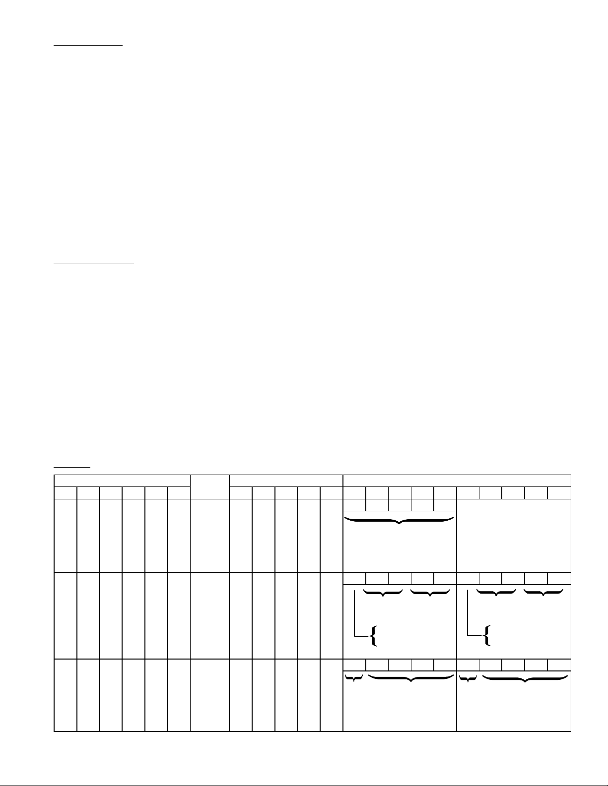
Table 1:
Control Word
C5 C4 C3 C2 C1 C0
0 0 0 0 0 0 1 LA LA LA LA LA E D C B A
0 0 0 0 0 1 1 LA LA LA LA M
0 0 0 0 1 1 1 LA LA LA M M
0 0 0 1 1 1 1 LA LA M M M
0 0 1 1 1 1 1 LA M M M M
0 1 1 1 1 1 1 M M M M M
0 0 1 0 Z Z 2 – S/R S/R S/R S/R 0 Y Y Z Z 1 Y Y Z Z
0 1 0 0 Z Z 2 – S/R S/R S/R M
0 1 0 1 Z Z 2 – S/R S/R M M
0 1 1 0 Z Z 2 – S/R M M M
1 0 Z Z Z Z 3 – LA LA LA LA 0 Z Z Z Z 1 D C B A
1 1 Z Z Z Z 3 – M M M M
Control
Mode
Output Response Interpretation pf PPM Words
E D C B A e d c b a e d c b a
PPM decoded
on all outputs
on all outputs
immediately
Output Receiver
Output Receiver
Output
address
Resets an S/R
type output
Address Receiver
Address
mode
Receiver
address
Receiver
address
Output
address
Sets an S/R type
output or pulses a
momentary outputmomentary output
Data PPM data sent
Data
mode
PPM data sent
Receiver
address
to outputs of
addressed
receiverreceiver

Notes:
1. Control Mode 1: Direct Response to the PPM Code
2. Control Mode 2: ZZ is a 2 bit address for the receiver
YY selects one of 4 outputs
YY OUTPUT
00 A
01 B
10 c
11 D
3. Control Mode 3: ZZZZ is a 4 bit address that selects, by which of 16PPM codes a receiver will be selected.
If PPM bit e = “1”, the rest of that PPM word will be read as data. If PPM bit e = “0”, the rest of that PPM word will be
read as an address.
Pin Connection Diagram
V
OSC Time Constant
PPM Input
Control Inputs
1
2
3
C0
4
C1
5C2
6C3
7C4
8C5
V
DD
9 10
CC
18
Output Enable
17
1615A
B
C
14
13
12
11
Binary Outputs
D
E
Power ON Clear
Data Ready
18 10
19
.870 (22.1) Max
.250
(6.35)
.150
(3.8)
.125 (3.17) Min.100 (2.54)
.800 (20.3)
 Loading...