

NTE NTE1749 Datasheet

NTE1749
Integrated Circuit
Push–Pull Four Channel Driver
Description:
The NTE1749 is a quad push–pull driver capable of delivering output currents to 1A per channel.
Each channel is controlled by a TTL–compatible logic input and each pair of drivers (a full bridge) is
equipped with an inhibit input which turns off all four transistors. A separate supply input is provided
for the logic so that it may be run off a lower voltage to reduce dissipation.
Features:
D Output Current 1A Per Channel
D Peak Output Current 2A Per Channel (Non Repetitive)
D Inhibit Facility
D High Noise Immunity
D Separate Logic Supply
D Overtemperature Protection
Absolute Maximum Ratings:
Supply Voltage, V
Logic Supply Voltage, V
Input Voltage, V
Inhibit Voltage, V
Peak Output Current (Non–Repetitive, t = 5ms), I
Total Power Dissipation (T
Operating Junction Temperature Range, T
Storage Temperature Range, T
S
SS
I
inh
O
ground–pins
= +80°C), P
stg
D
J
Maximum Thermal Resistance, Junction–to–Case R
Thermal Resistance, Junction–to–Ambient, R
thJA
–40° to +150°C. . . . . . . . . . . . . . . . . . . . . . . . . . . . . . . . . .
–40° to +150°C. . . . . . . . . . . . . . . . . . . . . . . . . . . . . . . . . . . . . . . . . .
thJC
36V. . . . . . . . . . . . . . . . . . . . . . . . . . . . . . . . . . . . . . . . . . . . . . . . . . . . . . . . . . . . . . . . .
36V. . . . . . . . . . . . . . . . . . . . . . . . . . . . . . . . . . . . . . . . . . . . . . . . . . . . . . . . . . .
7V. . . . . . . . . . . . . . . . . . . . . . . . . . . . . . . . . . . . . . . . . . . . . . . . . . . . . . . . . . . . . . . . . . . .
7V. . . . . . . . . . . . . . . . . . . . . . . . . . . . . . . . . . . . . . . . . . . . . . . . . . . . . . . . . . . . . . . . . .
2A. . . . . . . . . . . . . . . . . . . . . . . . . . . . . . . . . . . . . .
5W. . . . . . . . . . . . . . . . . . . . . . . . . . . . . . . . . . . . . .
14°C/W. . . . . . . . . . . . . . . . . . . . . . . . . . . . .
80°C/W. . . . . . . . . . . . . . . . . . . . . . . . . . . . . . . . . . .
Electrical Characteristics
Parameter Symbol Test Conditions Min Typ Max Unit
: (Per Channel, V
= 24V, VSS = 5V, TA = +25°C, unless otherwise specified)
S
Supply Voltage V
Logic Supply Voltage V
Total Quiescent Supply Current I
Total Quiescent Logic Supply Current I
Input Low Voltage V
Input High Voltage V
Low Voltage Input Current I
High Voltage Input Current I
Inhibit Low Voltage V
Inhibit High Voltage V
S
SS
S
S
IL
IH
IL
IH
inhL
inhH
V
SS
– 36 V
4.5 – 36 V
Vi = L, IO = 0, V
Vi = H, IO = 0, V
V
= L – – 4 mA
inh
Vi = L, IO = 0, V
Vi = H, IO = 0, V
V
= L – 16 24 mA
inh
= H – 2 6 mA
inh
= H – 16 24 mA
inh
= H – 44 60 mA
inh
= H – 16 24 mA
inh
–0.3 – 1.5 V
VSS ≤ 7V 2.3 – V
ss
V
VSS > 7V 2.3 – 7 V
VIL = 1.5V – – –10 µA
2.3V ≤ VIH ≤ VSS – 0.6V – 30 100 µA
–0.3 – 1.5 V
VSS ≤ 7V 2.3 – V
ss
V
Vss > 7V 2.3 – 7 V
Low Voltage Inhibit Current I
High Voltage Inhibit Current I
Source Output Saturation Voltage V
Sink Output Saturation Voltage V
Rise Time t
Fall Time t
Turn–On Delay Time t
Turn–Off Delay Time t
inhL
IHhH
CEsatHIO
CEsat LIO
r
f
on
off
Truth Table
Vi (Each Channel) V
H H H
L L H
H X (Note 1) L
L X (Note 1) L
o
V
inh
(Note 2)
Note 1. High Output Impedance
Note 2. Relative to the Considerate Channel
V
= 1.5V – –30 100 µA
inhL
2.3V ≤ V
≤ VSS –0.6V – – ±10 µA
inhH
= –1A – 1.4 1.8 V
= 1A – 1.2 1.8 V
0.1 to 0.9 V
0.9 to 0.1 V
o
o
0.5 Vi to 0.5 V
0.5 Vi to 0.5 V
o
o
– 250 – ns
– 250 – ns
– 750 – ns
– 200 – ns
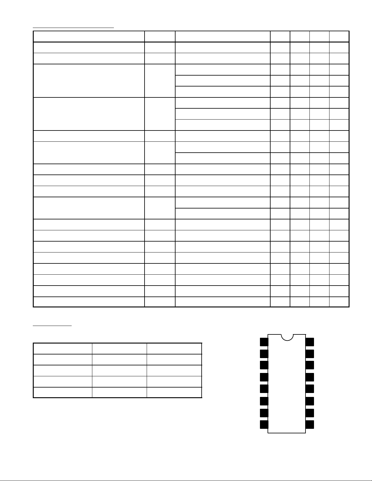
Pin Connection Diagram
CE 1
Input 1
Output 1
GND
1
2
3
4
5GND
6Output 2
7Input 2
V
8 9 CE 2
S
16
V
SS
15
Input 4
14
Output 4
13
GND
12 GND
11 Output 3
10 Input 3
 Loading...