

NTE NTE1745 Datasheet

NTE1745
Integrated Circuit
High Speed Divider 1/20, 1/100 for VCR
Description:
The NTE1745 is a semiconductor integrated circuit in an 8–Lead SIP type package consisting of a
built–in 1/20 and 1/100 high–speed frequency divider featuring an ECL circuit configuration.
Features:
D High–Speed Operation (f
D Operation at Low Input Amplitudes (180mV
= 130MHz)
max
Minimum Input Amplitude)
p–p
D TTL Level Output
Applications:
FM radio prescalers, digital equipment for consumer and industrial applications
Function:
This divider is based on an ECL circuit configuration. When a frequency up to a maximum of 130MHz
is applied to the TI input pin, 1/20–divided output is produced when the division ratio selection input
pin (M) is low–level or a 1/100–divided output is produced when the division ratio selection input pin
(M) is high–level. The output (TO) is available in the TTL level open collector format.
Absolute Maximum Ratings: (TA = –10° to +75°C unless otherwise specified)
Supply Voltage, V
Input Signal Voltage, V
Output Signal Voltage, V
CC
. . . . . . . . . . . . . . . . . . . . . . . . . . . . . . . . . . . . . . . . . . . . . . . . . . . . . . . . .
I
O
Power Dissipation (TA = +25°C), P
Operating Temperature Range, T
Storage Temperature Range, T
stg
opr
D
–10° to +75°C. . . . . . . . . . . . . . . . . . . . . . . . . . . . . . . . . . . . . . . .
–55° to +125°C. . . . . . . . . . . . . . . . . . . . . . . . . . . . . . . . . . . . . . . . .
1.5V
5.5V. . . . . . . . . . . . . . . . . . . . . . . . . . . . . . . . . . . . . . . . . . . . . . . . . . . . . . . . . .
1.33W. . . . . . . . . . . . . . . . . . . . . . . . . . . . . . . . . . . . . . . . . . . . . . .
9V. . . . . . . . . . . . . . . . . . . . . . . . . . . . . . . . . . . . . . . . . . . . . . . . . . . . . . . . . . . . . . . . .
p–p
Electrical Characteristics: (TA = –10° to +75°C unless otherwise specified)
Parameter Symbol Test Conditions Min Typ Max Unit
Supply Voltage V
Low–Level Output Current I
Input Frequency f
High Input Voltage (M Input) VIH(M) 2.6 – V
Low Input Voltage (M Input) VIL(M) 0 – 0.4 V
Input Signal Voltage V
Circuit Current I
Low–Level Output Voltage V
Minimum Operating Frequency f
High Input Current (M Input) I
Low Input Current (M Input) I
Output Leakage Current I
CC
OL
TA = +25°C 30 – 130 MHz
IN
TA = +25°C 180 – 800 mV
i
VCC = 5V – 6.5 – mA
CC
VCC = 4.5V, IOL = 5mA – – 0.5 V
OL
max
IH(M)
IL(M)
O(Leak)VCC
VCC = 5V, TA = +25°C, VIN = 180mV
VCC = 5V, VIH(M) = 2.6V – 2 – µA
VCC = 5V, VIL(M) = 0.4V – 0.1 – µA
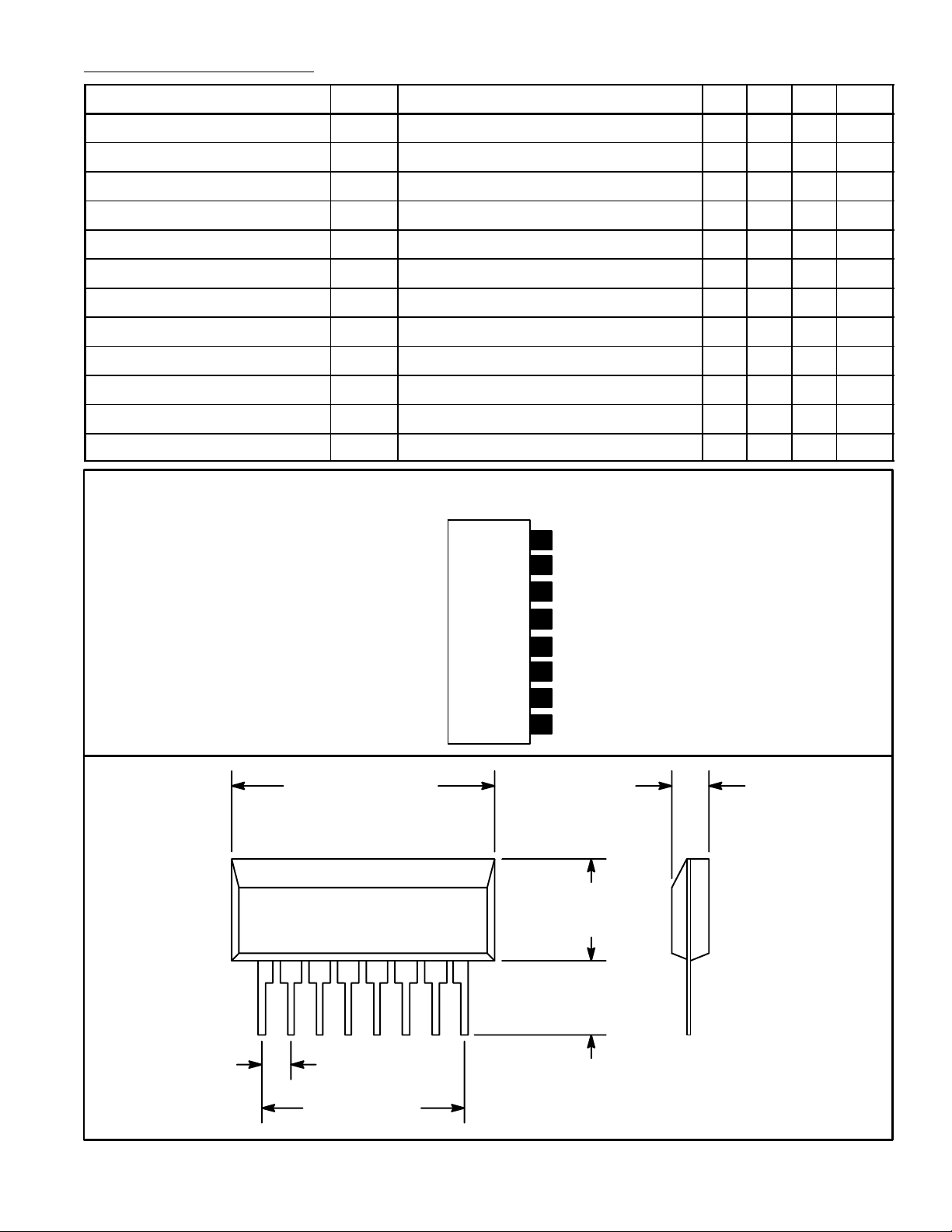
Pin Connection Diagram
p–p
= 5V, VO = 5.5V – – 100 µA
(Front View)
To Open Collector Output
8
7
V
CC
N.C.
6
4.5 5 5.5 V
– – 5 mA
cc
130 – – MHz
V
p–p
5
V
Input Reference Bias
ref
Input (T)
4
Frequency Division Ratio
3
Selection Input (M)
N.C.
2
GND
1
.768 (19.52) Max
18
.100 (2.54) Typ
.118 (3.0) Max
.264 (6.72)
Max
.165
(4.2)
Min
.700 (17.78)
 Loading...