

NTE NTE1735 Datasheet
NTE1735
Integrated Circuit
Module, 3 Output Positive Voltage
Regulator for VCR
Features:
D 3 Outputs
D Cutoff Function
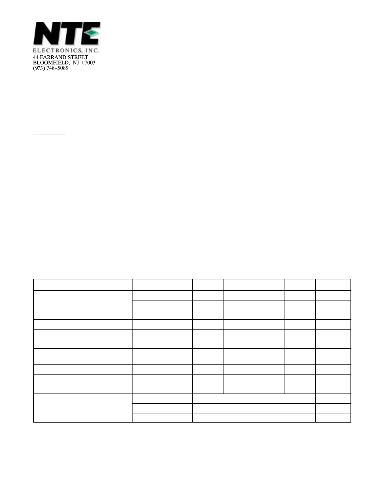
Absolute Maximum Ratings: (TA = +25°C unless otherwise specified)
Maximum DC Input Voltage, VIN (DC) Max
VO1 40V. . . . . . . . . . . . . . . . . . . . . . . . . . . . . . . . . . . . . . . . . . . . . . . . . . . . . . . . . . . . . . . . . . . . . . . .
VO2, VO3, VO4 35V. . . . . . . . . . . . . . . . . . . . . . . . . . . . . . . . . . . . . . . . . . . . . . . . . . . . . . . . . . . . . . .
Maximum Average Output Current, IO Max
VO1, VO 2 1.0A. . . . . . . . . . . . . . . . . . . . . . . . . . . . . . . . . . . . . . . . . . . . . . . . . . . . . . . . . . . . . . . . . .
VO3, VO 4 1.5A. . . . . . . . . . . . . . . . . . . . . . . . . . . . . . . . . . . . . . . . . . . . . . . . . . . . . . . . . . . . . . . . . .
Maximum Peak Output Current (0.2sec max), IO Max 2.5A. . . . . . . . . . . . . . . . . . . . . . . . . . . . . . . . . .
Operating Case Temperature, TC Max +105°C. . . . . . . . . . . . . . . . . . . . . . . . . . . . . . . . . . . . . . . . . . . . .
Junction Temperature, TJ Max +150°C. . . . . . . . . . . . . . . . . . . . . . . . . . . . . . . . . . . . . . . . . . . . . . . . . . . .
Storage Temperature Range, T
stg
Thermal Resistance, Junction–to–Case, R
thJC
–30° to +105°C. . . . . . . . . . . . . . . . . . . . . . . . . . . . . . . . . . . . . . . . . .
4.5°C/W. . . . . . . . . . . . . . . . . . . . . . . . . . . . . . . . . . . . .
Electrical Characteristics: (TA = +25°C unless otherwise specified)
Parameter Test Conditions VO1 VO2 VO3 VO4 Unit
Output Voltage Setting Condition 1, Note 1 16.0 ±0.3 – 12.0±0.1 11.9±0.1 V
Condition 1, Note 2 – 12.0±0.3 12.0±0.1 11.9±0.1 V
Ripple Voltage Condition 2 20 20 5 5 mV
Temperature Coefficient Condition 1 0.02 0.05 0.02 0.02 %/°C Max
Input Regulation Condition 3 35 50 35 35 mV/V Max
Load Regulation Condition 4 40 100 35 35 mV/A Max
Minimum Input–Output Voltage
Difference
Minimum Output Current – – – 10 mA Min
VO1/VO2 Select Condition 1, Note 1 ON – – –
Output ON Condition 1, Note 1 VO1 or VO2, VO3 ON
Condition 5 2.5 1.2 1.2 1.2 V Max
Condition 1, Note 2 – ON – –
Condition 1, Note 2 VO1 or VO2, VO3 OFF
Condition 1, Note 3 VO4 is always ON
p–p
Max
Note 1. Pin11 or Pin13 is at High Level (3V to 15V).
Note 2. Pin11 or Pin13 is at Low Level (≤ 1.2V).
Note 3. Pin11 or Pin13 is at High Level, Pin14 is at Low Level
Test Conditions:
Condition 1: VIN (DC) 1 = 21V, VIN (DC) 2 = 16V, IO1 or IO2 = IO4 = 0.5A, IO3 = 0.8A
Condition 2: V
(DC) 1 = 21V, VIN (DC) 2 = 16V, IO1 or IO2 = IO4 = 0.5A, IO3 = 0.8A,
IN
Input Ripple Voltage = 1.5V
P–P
Condition 3: VIN (DC) 1 = 19V to 25V, VIN (DC) 2 = 14V to 18V, IO1 or IO2 = IO4 = 0.5A, IO3 = 0.8A
Condition 4: V
Condition 5: I
(DC) 1 = 21V, VIN (DC) 2 = 16V, IO1 or IO2 = IO3 = IO4 = 0.2A to 2.5A
IN
1 or IO2 = IO4 = 0.5A, IO3 = 0.8A
O
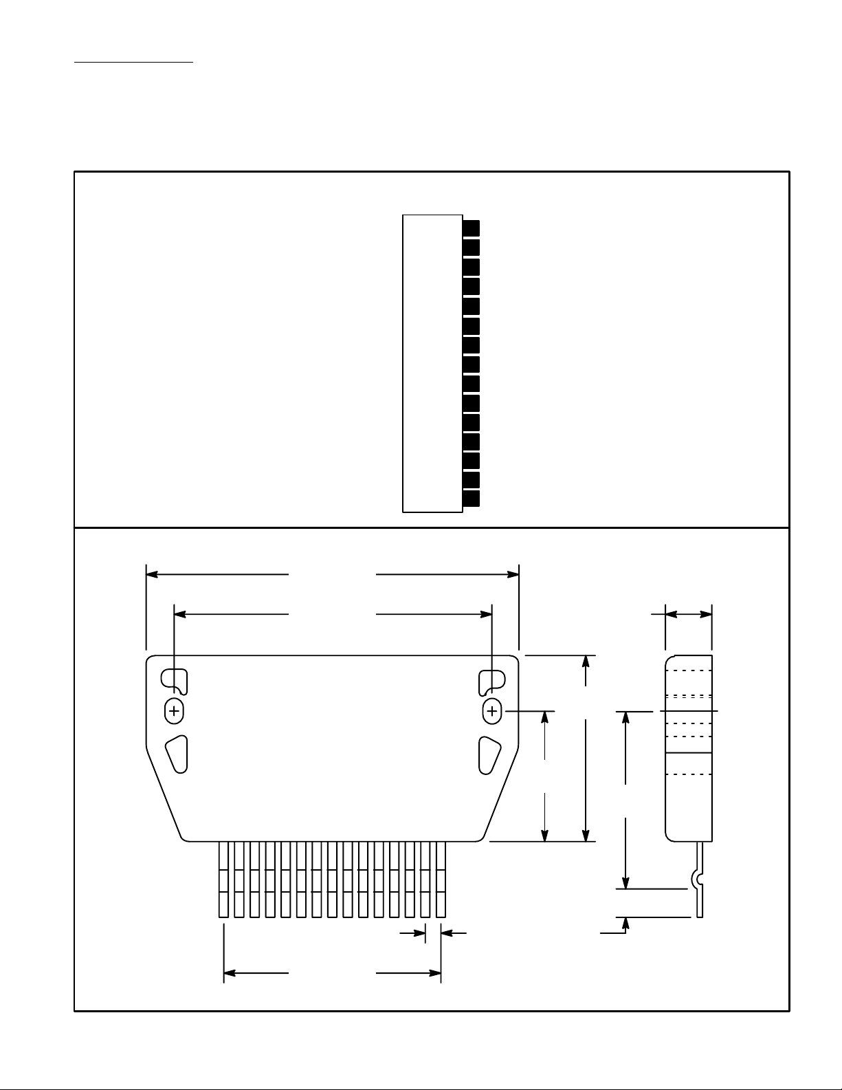
Pin Connection Diagram
(Front View)
15
Reference Input
H Switch
14
13
ON/OFF Control
GND
12
11 M Start
VIN (DC) 1
10
VIN (DC) 2
9
Reference Input
8
VO 1 (16V @ 1A)
7
VO 2 (12V @ 1A)
Reference Input
6
VO 3 (12V @ 1.5A)
5
Reference Input4
VIN (DC) 2
3
Control Voltage
2
VO 4 (11.9V @ 1.5A)
1
2.330 (59.2)
2.050 (52.0)
.827
(21.0)
115
.100 (2.54)
.158 (4.0)
.335 (8.5)
1.230
(31.2)
1.110
(28.0)
1.400 (35.6)
 Loading...