

NTE NTE1732 Datasheet

NTE1732
Integrated Circuit
Module, Hybrid, TV Voltage Regulator
w
/4W Audio Output
Features:
D Series Regulator and Audio Output Amp Incorporated into a Single Package
D Low Power Dissipation, Low Distortion, High Gain
D Excellent Heat Radiation and Thermal Stability
Functions:
D Line Operated Series Regulator
D Line Operated Audio Output Amp
Applications:
D NTSC System Color Television Sets
Absolute Maximum Ratings:
Maximum Input Voltage (Between Pin1 and Pin4), V
(TA = +25°C unless otherwise specified)
max 200V. . . . . . . . . . . . . . . . . . . . . . . . . . . . . .
in
Maximum Supply Voltage (Between Pin8 and Pin11), V
Maximum Output Current (Pin6), I
Maximum Collector Output Current (TR5, TR6), I
Operating Case Temperature, T
Operating Junction Temperature, T
Storage Temperature Range, T
Thermal Resistance, Junction–to–Case (TR1), R
max 1A. . . . . . . . . . . . . . . . . . . . . . . . . . . . . . . . . . . . . . . . . . . . . . . .
O
max 1A. . . . . . . . . . . . . . . . . . . . . . . . . . . . . . . . . . .
C
C
J
stg
thJC1
Thermal Resistance, Junction–to–Case (TR5, TR6), R
Allowable Load Shorting Time (V
= 158V, RL = 8Ω, PO = 1W, f = 50Hz), t
indc
max 160V. . . . . . . . . . . . . . . . . . . . . . . . . .
CC
–30° to +105°C. . . . . . . . . . . . . . . . . . . . . . . . . . . . . . . . . . . . . . . . . .
thJC2
s
+105°C. . . . . . . . . . . . . . . . . . . . . . . . . . . . . . . . . . . . . . . . . . . . . . . . . .
+150°C. . . . . . . . . . . . . . . . . . . . . . . . . . . . . . . . . . . . . . . . . . . . . . .
1.8°C/W. . . . . . . . . . . . . . . . . . . . . . . . . . . . . . .
12.5°C/W. . . . . . . . . . . . . . . . . . . . . . . . .
2sec. . . . . . . . . . . . .
Electrical Characteristics: (TA = +25°C unless otherwise specified)
Parameter Symbol Test Conditions Min Typ Max Unit
Power Supply Block
Output Voltage V
Output Voltage Fluctuation
Against Input Voltage
Against Output Current V
Output Voltage Temperature Factor V
Ripple Compression Rate Vac = 120V, IO= 0.5A – 37 – dB
Withstanding Voltage Between
Input and Output Pins
Saturation Voltage Between
Input and Output Pins
DC Current Gain h
Audio Output (V
Quiescent Current I
Output Power P
Total Harmonic Distortion THD PO = 0.1W, f = 1kHz – – 2 %
Voltage Gain V
Frequency Response fL, f
Output Noise Voltage V
Middle–Point Voltage V
= 158V, IO = 200mA, Rg = 600Ω, RL2 = 440Ω unless otherwise specified)
indc
CCO
V
O
FE
O
G
H
NO
N
= 158V, IO = 0.5A, Note 1 134.2 135.2 136.2 V
indc
V
= 151V to 174V, IO = 0.5A –1 – +1 V
indc
= 158V, IO = 0.2A to 0.5A – – 0.5 V
indc
= 158V, IO = 0.5A – 7 – mV/°C
indc
TR1, I
TR1, IB = 10mA, IC = 1A – – 0.2 V
TR1, VCE = 5V, IC = 1A 1500 – 6500
V
indc
THD = 10%, f = 1kHz 4.0 5.0 – W
PO = 0.1W, f = 1kHz 47 49 51 dB
PO = 0.1W, ±6dB 70 to 10k Hz
Rg = 0Ω – – 2.0 mV
Pin9 66.5 68.5 70.5 V
= 10mA – 200 – V
CEO
= 135V, Pin6 3 5 10 mA
Note 1. Measure within 5 min. after switch is on.
Note 2. Unless otherwise specified, voltage regulated power supply is used.
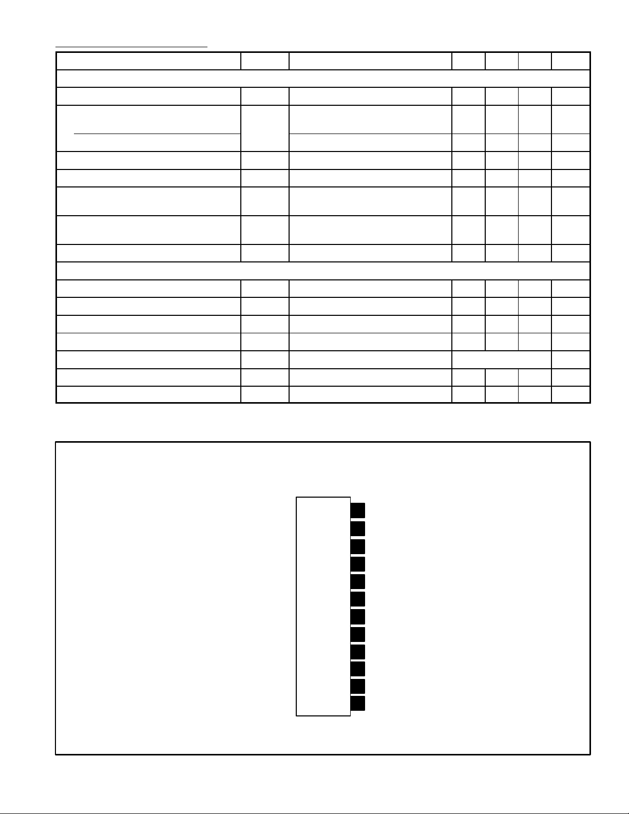
Pin Connection Diagram
(Front View)
AF Input
12
GND
11
Bypass
10
AF Output
9
Bias Resistor
8
Bootstrap
7
Reg Voltage Output
6
No Pin
5
(–) DC Input
4
3
No Pin
Reg Drive
2
(+) DC Input
1
 Loading...