

NTE NTE1729 Datasheet
NTE1729
Integrated Circuit
Pulse Width Modulator (PWM) Control Circuit
Description:
The NTE1729 is an inverter control unit in a 16–Lead DIP type package which provides all the control
circuitry for PWM type switching regulators. Included in this device is the voltage reference, dual error
amplifiers, oscillator, pulse width modulator, pulse steering flip flop, dual alternating output switches,
and dead time control.
Features:
D Complete PWM Power Control Circuit
D Adjustable Dead Time: 0 to 100%
D No Double Pulsing of Same Output during Load Transient Condition
D Dual Error Amplifiers have Wide Common Mode Input Voltage Capability: –0.3V to VCC –2V
D Circuit Architecture Provides Easy Synchronization
D Uncommitted Outputs for 250mA Sink or Source
D With Miss–Operation Prevention Circuit for Low Level Supply Voltage
Absolute Maximum Ratings: (TA = +25°C unless otherwise specified)
Supply Voltage, VCC 41V. . . . . . . . . . . . . . . . . . . . . . . . . . . . . . . . . . . . . . . . . . . . . . . . . . . . . . . . . . . . . . .
Error Amplifier Input Voltage, V
Output Voltage, V
41V. . . . . . . . . . . . . . . . . . . . . . . . . . . . . . . . . . . . . . . . . . . . . . . . . . . . . . . . . . . . . .
CER
Total Power Dissipation (TA = +25°C), P
Operating Temperature Range, T
Storage Temperature Range, T
V
ICM
T
opr
–65° to +150°C. . . . . . . . . . . . . . . . . . . . . . . . . . . . . . . . . . . . . . . . . .
stg
–20° to +85°C. . . . . . . . . . . . . . . . . . . . . . . . . . . . . . . . . . . . . . . . .
CC
1000mW. . . . . . . . . . . . . . . . . . . . . . . . . . . . . . . . . . . . . . . . .
+0.3V. . . . . . . . . . . . . . . . . . . . . . . . . . . . . . . . . . . . . . . . . . . . .
Recommended Operating Conditions:
Parameter Symbol Min Typ Max Unit
Supply Voltage V
Output Voltage V
Output Current I
Error Amplifier Sink Current I
Timing Capacitor C
Timing Resistance R
Oscillation Frequency f
Operating Temperature T
CC
CER
C
OAMP
T
T
osc
opt
7 – 40 V
–0.3 – 40 V
– – 200 mA
– – –0.3 mA
0.47 – 10000 nF
1.8 – 500 kΩ
1 – 300 kHz
–20 – +70 °C
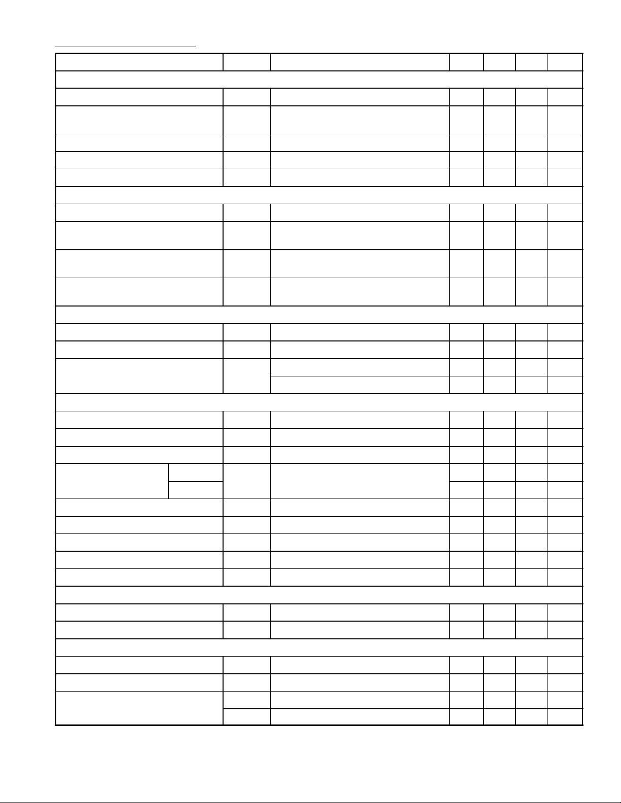
Electrical Characteristics: (VCC = +15V, f = 10kHz, –20° ≤ TA ≤ +70°C, unless otherwise spe cifie d)
Parameter Symbol Test Conditions Min Typ Max Unit
Reference Section
Output Voltage V
Line Regulation REG
I
ref
ref
7V ≤ VCC ≤ 40V, I
IN
= 1mA, TA = +2 5°C 4.75 5.0 5.25 V
= 1mA,
ref
– 8 25 mV
TA = +2 5°C
Load Regulation REGL1mA ≤ I
Temperature Coefficient V
Short–Circuit Output Current I
short
–20° ≤ TA ≤ +85°C, I
ref
V
ref
≤ 10mA, TA = +2 5°C – 1 15 mV
ref
= 1mA – 0.01 0.03 %/°C
ref
= 0, TA = +2 5°C, Note 2 – 50 – mA
Oscillator Section
Frequency f
OSC
Standard Deviation of Frequency 7V ≤ VCC ≤ 40V, CT, RT, Const.,
CT = 0.01µF, RT = 12kΩ, TA = +2 5°C – 10 – kHz
– 10 – %
TA = +2 5°C, Note 1
Frequency Change with Temperature 0° ≤ TA ≤ +70°C, CT = 0.01µF,
– 1 2 %
RT = 12kΩ
Frequency Change with Voltage 7V ≤ VCC ≤ 40V, CT = 0.01µF,
– – 1 %
RT = 12kΩ, TA = +2 5°C
Dead–Time Control Section
Input Bias Current 0 ≤ VI ≤ 5.25V – –2 –10 µA
Maximum Duty Cycle (Each Output) VI = 0 45 49 – %
Input Threshold Voltage V
Zero Duty Cycle – 3.0 3.3 V
th
Maximum Duty Cycle 0 – – V
Error Amplifier Section
Input Offset Voltage V
Input Offset Current I
IO
Input Bias Current V
Common Mode Input
Voltage
Low
V
ICM
High V
Open–Loop Voltage Amplification A
V
IO
V
7V ≤ VCC ≤ 40V
V
V
= 2.5V – 2 10 mV
OAMP
= 2.5V – 25 250 nA
OAMP
= 2.5V – 0.2 1.0 mA
OAMP
–0.3 – – V
–2
CC
= 0.5V to 3.5V, TA = +2 5°C 60 80 – dB
OAMP
– – V
Unity Gain Bandwidth TA = +2 5°C 500 830 – kHz
Common Mode Rejection Ratio CMRR VCC = 40V, TA = +2 5°C 65 80 – dB
Output Sink Current V
Output Source Current V
= 0.7V 0.3 0.7 – mA
OAMP
= 3.5V –2 –10 – mA
OAMP
PWM Section
Input Threshold Voltage Zero Duty Cycle – 4.0 4.5 V
Input Sink Current V
= 0.7V 0.3 0.7 – mA
(Pin3)
Output Section
Collector Cutoff Current I
CER
VCE = 40V, VCC = 40V – 2 100 µA
Emitter Cutoff Current VCC = VC = 40V – – –100 µA
Collector Saturation Voltage V
CE(sat)IC
V
CE(on)IE
= 200mA, VE = 0, Common Emitter 0 0.95 1.3 V
= 200mA, VC = 15V, Emitter Follower – 1.6 2.5 V
 Loading...