

NTE NTE1721, NTE1723 Datasheet

NTE1721 & NTE1723
Integrated Circuit
Pulse Width Modulator (PWM) Regulator
Description:
The NTE1721 and NTE1723 are pulse width modulator control–circuits designed to offer improved
performance and lowered external parts count when implemented for controlling all types of switching
power supplies. The no–chip +5.1V reference is trimmed to ±1% and the input common–mode range
of the errror amplifier includes the reference voltage, thus eliminating the need for external divider
resistors. A sync input to the oscillator enables multiple units to be slaved or a single unit to be synchronized to an external system clock. A wide range of dead time can be programmed by a single
resistor connected between the CT and the Discharge pins. These devices also feature a built–in
soft–start circuitry, requiring only an external timing capacitor. A shutdown pin controls both the soft–
start circuitry and the output stages, provided instantaneous turn–off through the PWM latch with
pulsed shutdown, as well as soft–start recycle with longer shutdown commands. The under voltage
lockout inhibits the outputs and the changing of the soft–start capacitor when VCC is below nominal.
The output stages are totem–pole design capable of sinking and sourcing in excess of 200mA. The
output stages of the NTE1721 features NOR logic resulting in a low output for an off state while the
NTE1723 utilizes OR logic which gives a high output when off.
Features:
D 8V to 35V Operation
D +5.1V ±1% Trimmed Reference
D 100Hz to 400kHz Oscillator Range
D Separate Oscillator Sync Pin
D Adjustable Dead Time Control
D Input Undervoltage Lockout
D Latching PWM to Prevent Multiple Pulses
D Pulse–by–Pulse Shutdown
D Dual Source/Sink Outputs: ±400mA Peak
Absolute Maximum Ratings: (Note 1)
Supply Voltage, VCC +40V. . . . . . . . . . . . . . . . . . . . . . . . . . . . . . . . . . . . . . . . . . . . . . . . . . . . . . . . . . . . . .
Collector Supply Voltage, V
C
+40V. . . . . . . . . . . . . . . . . . . . . . . . . . . . . . . . . . . . . . . . . . . . . . . . . . . . . . . .
Logic Inputs –0.3V to +5.5V. . . . . . . . . . . . . . . . . . . . . . . . . . . . . . . . . . . . . . . . . . . . . . . . . . . . . . . . . . . . .
Analog Inputs –0.3V to V
Output Current, Source or Sink, I
Reference Output Current, I
. . . . . . . . . . . . . . . . . . . . . . . . . . . . . . . . . . . . . . . . . . . . . . . . . . . . . . . . . . . . . .
O
ref
±500mA. . . . . . . . . . . . . . . . . . . . . . . . . . . . . . . . . . . . . . . . . . . . . . . .
50mA. . . . . . . . . . . . . . . . . . . . . . . . . . . . . . . . . . . . . . . . . . . . . . . . . . . . .
Oscillator Charging Current 5mA. . . . . . . . . . . . . . . . . . . . . . . . . . . . . . . . . . . . . . . . . . . . . . . . . . . . . . . . .
Power Dissipation (TA = +25°C), P
D
1000mW. . . . . . . . . . . . . . . . . . . . . . . . . . . . . . . . . . . . . . . . . . . . .
Derate Above 50°C 10mW/°C. . . . . . . . . . . . . . . . . . . . . . . . . . . . . . . . . . . . . . . . . . . . . . . . . . . . . .
Power Dissipation (TC = +25°C), P
D
2000mW. . . . . . . . . . . . . . . . . . . . . . . . . . . . . . . . . . . . . . . . . . . . .
Derate Above 25°C 16mW/°C. . . . . . . . . . . . . . . . . . . . . . . . . . . . . . . . . . . . . . . . . . . . . . . . . . . . . .
Operating Junction Temperature, T
Storage Temperature Range, T
Thermal Resistance, Junction–to–Ambient, R
Thermal Resistance, Junction–to–Case, R
J
stg
thJA
thJC
Lead Temperature (During Soldering, 10sec), T
–55° to +125°C. . . . . . . . . . . . . . . . . . . . . . . . . . . . . . . . . . . . . . . . . .
L
+150°C. . . . . . . . . . . . . . . . . . . . . . . . . . . . . . . . . . . . . . . . . . . . . . .
100°C/W. . . . . . . . . . . . . . . . . . . . . . . . . . . . . . . . . .
60°C/W. . . . . . . . . . . . . . . . . . . . . . . . . . . . . . . . . . . . . .
+300°C. . . . . . . . . . . . . . . . . . . . . . . . . . . . . . . . . . . .
Note 1 Values beyond which damage may occur
CC
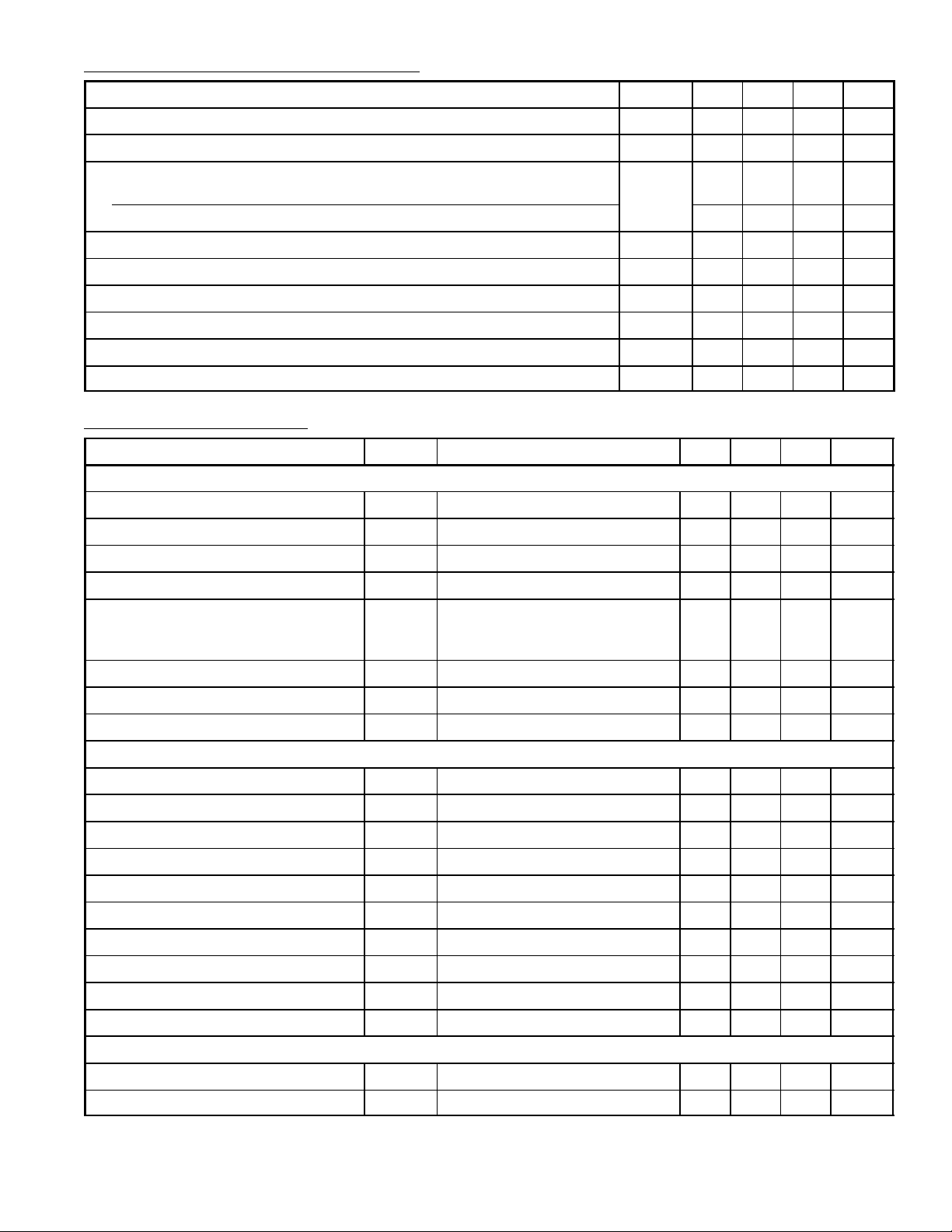
Recommended Operating Conditions:
Parameter Symbol Min Typ Max Unit
Supply Voltage V
Collector Supply Voltage V
Output Sink/Source Current
Steady State
I
CC
C
O
8.0 – 35.0 V
4.5 – 35.0 V
0 – ±100 mA
Peak 0 – ±400 mA
Reference Load Current I
Oscillator Frequency Range f
Oscillator Timing Resistor R
Oscillator Timing Capacitor C
Deadtime Resistor Range R
Operating Ambient Temperature Range T
ref
osc
T
T
D
A
0 – 20 mA
0.1 – 400 kHz
2.0 – 150 kΩ
0.001 – 0.2 µF
0.5 – – Ω
0 – 70 °C
Electrical Characteristics: (VCC = +20V, TA = 0° to +70°C unless otherwise specified)
Parameter Symbol Test Conditions Min Typ Max Unit
Reference Section
Reference Output Voltage V
Line Regulation Reg
Load Regulation Reg
Temperature Stability ∆V
Total Output Variation (Includes Line
ref
∆V
and Load Regulation over
Temperature
TJ = +25°C 5.0 5.1 5.2 V
ref
+8V ≤ VCC ≤ +35V – 10 20 mV
line
0mA ≤ IL ≤ 20mA – 20 50 mV
load
/∆T – 20 – mV
ref
4.95 – 5.25 V
Short Circuit Current I
Output Noise Voltage V
SC
V
= 0V, TJ = +25°C – 80 100 mA
ref
10Hz ≤ f ≤ 10kHz, TJ = +25°C – 40 200 µV
n
rms
Long Term Stability S TJ = +25°C, Note 2 – 20 50 mV/kHr
Oscillator Section (Tested at f
= 40kHz, RT = 3.6kΩ, CT = 0.001µF, RD = 0Ω unless otherwise specified)
osc
Initial Accuracy TJ = +25°C – ±2 ±6 %
Frequency Stability with Voltage f
osc/VCC
Frequency Stability with Temperature f
Minimum Frequency f
Maximum Frequency f
osc
min
max
+8V ≤ VCC ≤ +35V – ±1 ±2 %
/T – ±3 – %
RT = 150kΩ, CT = 0.2µF – 50 – Hz
RT = 2kΩ, CT = 1.0nF 400 – – kHz
Current Mirror IRT = 2mA 1.7 2.0 2.2 mA
Clock Amplitude 3.0 3.5 – V
Clock Width TJ = +25°C 0.3 0.5 1.0 µs
Sync Threshold 1.2 2.0 2.8 V
Sync Input Current Sync Voltage = +3.5V – 1.0 2.5 mA
Error Amplifier Section (VCM = +5.1V)
Input Offset Voltage V
Input Bias Current I
IO
IB
– 2.0 10.0 mV
– 1.0 10.0 µA
Note 2. Since long term stability cannot be measured on each device before shipment, this specifica-
tion is an engineering estimate of average stability from lot to lot.
 Loading...