

NTE NTE1722 Datasheet

NTE1722
Integrated Circuit
Pulse Width Modulator (PWM) Control Circuit
Description:
The NTE1722 is a high performance pulse width modulator integrated circuit in an 18–Lead DIP type
package intended for fixed frequency switching regulators and other power control applications.
Functions included in this IC are a temperature compensated voltage reference, sawtooth oscillator,
error amplifier , pulse width modulator, pulse metering and steering logic, and two high current totem
pole outputs ideally suited for driving the capacitance of power FETs at high speeds.
Additional protective features include soft start and undervoltage lockout, digital current limiting,
double pulse inhibit, adjustable dead time and a data latch for single pulse metering. All digital control
ports art TTL and B–series CMOS compatible. Active low logic design allows easy wired–OR connections for maximum flexibility. The versatility of this device enables implementation in single–ended
or push–pull switching regulators that are transformerless or transformer coupled.
Features:
D 8.0 to 35 Volt Operation
D 5.0 Volt ±1% Trimmed Reference
D 1.0Hz to 400kHz Oscillator Range
D Dual Source/Sink Current Outputs: ±100mA
D Digital Current Limiting
D Programmable Dead Time
D Wide Current Limit Common Mode Range
D Guaranteed 6 Unit Synchronization
Absolute Maximum Ratings: (Values beyond which damage may occur)
Supply Voltage, V
Collector Supply Voltage, V
CC
C
Logic Inputs –0.3 to +5.5V. . . . . . . . . . . . . . . . . . . . . . . . . . . . . . . . . . . . . . . . . . . . . . . . . . . . . . . . . . . . . .
Analog Inputs –0.3 to V
Output Current (Source or Sink), I
O
Reference Load Current (VCC = 40V, Note 1), I
ref
±200mA. . . . . . . . . . . . . . . . . . . . . . . . . . . . . . . . . . . . . . . . . . . . . .
Logic Sink Current 15mA. . . . . . . . . . . . . . . . . . . . . . . . . . . . . . . . . . . . . . . . . . . . . . . . . . . . . . . . . . . . . . . .
Power Dissipation (TA = +25°C), P
D
1000mW. . . . . . . . . . . . . . . . . . . . . . . . . . . . . . . . . . . . . . . . . . . . .
Derate Above 50°C 10mW/°C. . . . . . . . . . . . . . . . . . . . . . . . . . . . . . . . . . . . . . . . . . . . . . . . . . . . . .
Power Dissipation (TC = +25°C), P
D
3000mW. . . . . . . . . . . . . . . . . . . . . . . . . . . . . . . . . . . . . . . . . . . . .
Derate Above 25°C 24mW/°C. . . . . . . . . . . . . . . . . . . . . . . . . . . . . . . . . . . . . . . . . . . . . . . . . . . . . .
Operating Junction Temperature, TJ + 150°C. . . . . . . . . . . . . . . . . . . . . . . . . . . . . . . . . . . . . . . . . . . . . .
Storage Temperature Range, T
Thermal Resistance, Junction–to–Ambient, R
Lead Temperature (During Soldering, 10sec), T
–65° to +150°C. . . . . . . . . . . . . . . . . . . . . . . . . . . . . . . . . . . . . . . . . .
stg
thJA
L
100°C/W. . . . . . . . . . . . . . . . . . . . . . . . . . . . . . . . . .
±300°C. . . . . . . . . . . . . . . . . . . . . . . . . . . . . . . . . . . .
Note 1. Maximum junction temperature must be observed.
+40V. . . . . . . . . . . . . . . . . . . . . . . . . . . . . . . . . . . . . . . . . . . . . . . . . . . . . . . . . . . . . . .
+40V. . . . . . . . . . . . . . . . . . . . . . . . . . . . . . . . . . . . . . . . . . . . . . . . . . . . . . . .
V. . . . . . . . . . . . . . . . . . . . . . . . . . . . . . . . . . . . . . . . . . . . . . . . . . . . . . . . . . . . .
CC
50mA. . . . . . . . . . . . . . . . . . . . . . . . . . . . . . . . . . . . .
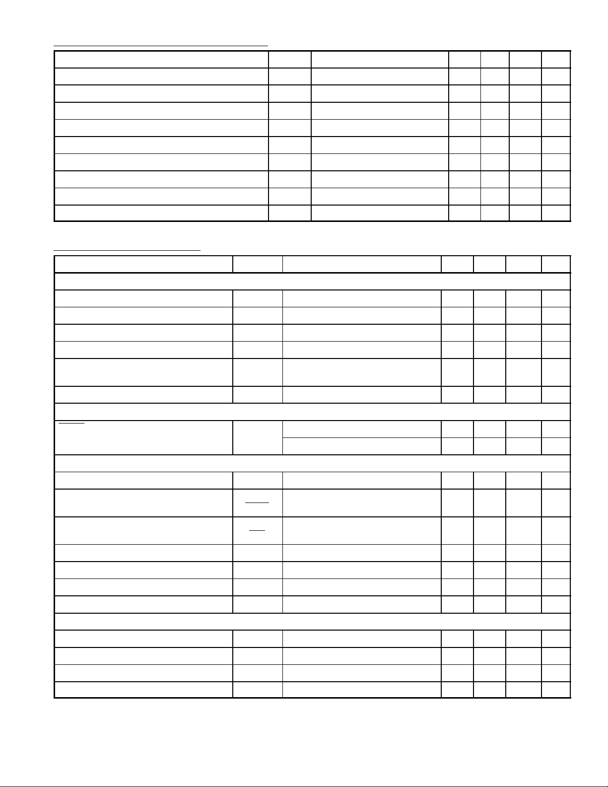
Recommended Operating Conditions:
Parameter Symbol Test Conditions Min Typ Max Unit
Supply Voltage V
Collector Supply Voltage V
Output Sink/Source Current (Each Output) I
Reference Load Current I
Oscillator Frequency Range I
Oscillator Timing Resistor R
Oscillator Timing Capacitor C
CC
C
O
ref
ref
T
T
+8.0 – +35 V
+4.5 – +35 V
0 – ±100 mA
0 – 20 mA
0 – 20 mA
2.0 – 150 kΩ
0.001 – 20 µF
Available Deadtime Range (40kHz) – 3.0 – 50 %
Operating Junction Temperature Range T
J
0 – +125 °C
Electrical Characteristics: (VCC = 15V, TJ = 0° to +125°C unless otherwise specified)
Parameter Symbol Test Conditions Min Typ Max Unit
Referencd Section (IL = 0mA unless otherwise specified)
Reference Output Voltage V
Line Regulation Reg
Load Regulation Reg
Temperature Stability ∆V
ref
Total Reference Output Voltage Variation ∆V
Short Circuit Current I
Uundervoltage Lockout
ref
SC
TJ = +25°C 4.90 5.00 5.10 V
+8.0V ≤ VCC ≤ +35V – 10 30 mV
line
0mA ≤IL ≤ 20mA – 10 50 mV
load
/∆T
J
+8.0V ≤ VCC ≤ +35V,
ref
– 10 – mV
4.85 5.00 5.15 V
0mA ≤ IL ≤ 20mA
V
= 0V, Note 1 25 80 125 mA
ref
Reset Output V oltage – V
= +3.8V – 0.2 0.4 V
ref
V
= +4.8V 2.4 4.8 – V
ref
Oscillator Section (Note 2)
Initial Accuracy – TJ = +25°C – ±3.0 ±8.0 %
Frequency Stability over Power
Supply Range
Frequency Stability over Temperature ∆f
Minimum Frequency f
Maximum Frequency f
Sawtooth Peak Voltage V
Sawtooth Valley Voltage V
∆f
∆V
∆T
min
max
osc(p)
osc(v)
osc
CC
osc
+8.0V ≤ VCC ≤ +35V – 0.5 1.0 %
∆TJ = 0° to +125°C – 2.0 – %
J
RT = 150kΩ, CT = 20µF – 0.5 – Hz
RT = 2kΩ, CT = 0.001µF 400 – – kHz
VCC = +35V – 3.0 3.5 V
VCC = +8V 0.45 0.8 – V
Error Amplifier Section (0V ≤ VCM ≤ +5.2V unless otherwise specified)
Input Offset Voltage V
Input Bias Current I
Input Offset Current I
DC Open Loop Gain A
IO
IB
IO
VOL
RS ≤ 2kΩ – 20 10 mV
– –350 –2000 nA
– 35 200 nA
RL ≥ 10MΩ 60 72 – dB
Note 1. Maximum junction temperature must be observed.
Note 2. f
= 40kHz (RT = 4.12kΩ ± 1%, CT = 0.01µF ± 1%, RD = 0Ω)
OSC
 Loading...