

NTE NTE1720 Datasheet

NTE1720
Integrated Circuit
Pulse Width Modulator (PWM) Regulator
Description:
The NTE1720 PWM switching regulator control circuit contains all the essential circuitry to implement
single–ended or push–pull switching regulators. Included on the circuit are oscillator, voltage reference, a pulse width modulator, error amplifier, overload protection circuitry and output drivers.
A substance zener reference has been used to provide excellent stability with time and the reference
has been used to provide excellent stability with time and the reference is trimmed at the wafer level
to provide an initial accuracy of 2%. Additionally, the oscillator is trimmed to provide a medium tolerance of 6%.
Features:
D Reference Tolerance: ±2%
D Oscillator Tolerance: ±6%
D Long Term Stability: 10mV/1000 Hrs
D Operates Above 100kHz
Applications:
D Switching Power Supplies
D Motor Speed Control
D Off–Line Power Converters
Absolute Maximum Ratings:
Input Voltage, V
I
40V. . . . . . . . . . . . . . . . . . . . . . . . . . . . . . . . . . . . . . . . . . . . . . . . . . . . . . . . . . . . . . . . . . .
Reference Output Current 50mA. . . . . . . . . . . . . . . . . . . . . . . . . . . . . . . . . . . . . . . . . . . . . . . . . . . . . . . . .
Output Current (Each Output) 100mA. . . . . . . . . . . . . . . . . . . . . . . . . . . . . . . . . . . . . . . . . . . . . . . . . . . . .
Oscillator Charging Current (Pin6 or Pin7) 5mA. . . . . . . . . . . . . . . . . . . . . . . . . . . . . . . . . . . . . . . . . . . .
Internal Power Dissipation (Note 1), P
Operating Temperature Range, T
Storage Temperature Range, T
stg
D
opr
Lead Temperature (During soldering, 10 sec), T
–55°C to +125°C. . . . . . . . . . . . . . . . . . . . . . . . . . . . . . . . . . . . . .
–65°C to +150°C. . . . . . . . . . . . . . . . . . . . . . . . . . . . . . . . . . . . . . . .
L
1W. . . . . . . . . . . . . . . . . . . . . . . . . . . . . . . . . . . . . . . . . . . . . . .
+300°C. . . . . . . . . . . . . . . . . . . . . . . . . . . . . . . . . . . .
Note 1. For operating at elevated temperatures, the NTE1720 is derated at 150°C/W to a maximum
junction temperature of 115°C.
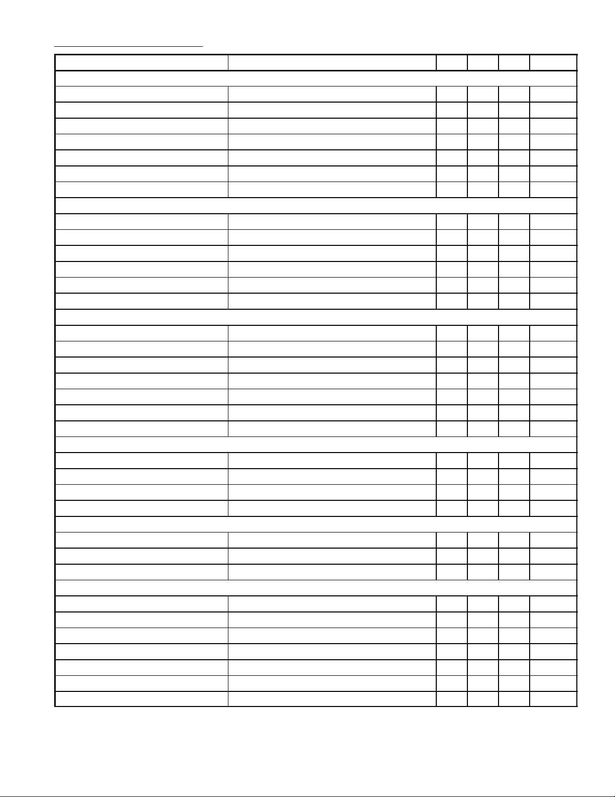
Electrical Characteristics: (TA = +25°C, VIN = 20V, f = 20kHz unless otherwise specified)
Parameter Test Conditions Min Typ Max Unit
Reference Section
Output Voltage 4.8 5.8 5.2 V
Line Regulation VIN = 8V to 40V – 10 20 mV
Load Regulation IL = 0mA to 20 – 20 50 mV
Ripple Rejection t = 120Hz – 66 – dB
Short Circuit Current Limit V
Temperature Stability – 0.3 1 %
Long Term Stability – 20 – mV/kHz
Oscillator Section
Maximum Frequency CT = 0.001pF, RT = 2kΩ – 300 – kHz
Initial Accuracy RT and CT Constant – 6 – %
Voltage Stability VIN = 8V to 40V – – 1 %
Temperature Stability – 2 – %
Output Amplitude Pin3 – 3.5 – µs
Output Pulse Width CT = 0.01µF, TA = 25°C – 0.5 – µs
Error Amplifier Section
Input Offset Voltage VCM = 2.5V – 0.5 5 mV
Input Bias Current VCM = 2.5V – 2 10 µA
Open Loop Voltage Gain 72 80 – dB
Common–Mode Voltage 1.8 – 3.4 V
Common–Mode Rejection Ratio – 70 – dB
Small Signal Bandwidth AV = 0dB – 3 – MHz
Output Voltage 0.5 – 3.8 V
Comparator Section
Minimum Duty Cycle – – 0 %
Maximum Duty Cycle 45 40 – %
Input Threshold Zero Duty Cycle – 1 – V
Input Bias Current – 1 – µA
Current Limiting Section
Sense Voltage Pin 9 = 2V with Error Amplifier Set for Max Out 180 200 220 mV
Sense Voltage T.C. – 0.2 – mV/°C
Common–Mode Voltage –1 – 1 V
Output Section (Each Output)
Collector–Emitter Voltage 40 – – V
Collector Leakage Current VCE = 40V – 0.1 50 µA
Saturation Voltage IC = 50mA – 1 2 V
Emitter Output Voltage VIN = 20V 17 16 – V
Rise Time RC = 2kΩ – 0.2 – µs
Fall Time RC = 2kΩ – 0.1 – µs
Total Standby Current VIN = 40V, Note 2 – 8 10 mA
= 0 – 100 – mA
REF
Note 2. Standby current does not include the oscillator charging current, error and current limit divid-
ers, and the outputs are open circuit.
 Loading...