


NTE1716
Integrated Circuit
Reversible Motor Driver for VCR
Features:
D Supply Voltage Range: 6V to 18V
D Power Dissipation: 2200mW
D Output Motor Driving Current up to 1600mA
D Two Control Logic Inputs Allow Switching of Three Output States:
Forward
Reverse
Braking
D Low Standby Current
D Adjustable Output Voltage Enables Motor Speed Control Using Control Pin Voltage
D Interfaces with CMOS Devices
D Built–In Components to Absorb Motor Rush Currents
Applications:
D Video Tape Recorders
D Cassette Tape Recorders
Absolute Maximum Ratings: (TA = +25°C unless otherwise specified)
Supply Voltage, V
Power Dissipation (TA = +25°C), P
CC
D
Derate Above +25°C 22mW/°C. . . . . . . . . . . . . . . . . . . . . . . . . . . . . . . . . . . . . . . . . . . . . . . . . . . . .
Output Current (Pulse Width = 500µs, Duty Cycle = 1%), I
Input Voltage, V
Operating Temperature Range, T
Storage Temperature Range, T
. . . . . . . . . . . . . . . . . . . . . . . . . . . . . . . . . . . . . . . . . . . . . . . . . . . . . . . . . .
IN
opr
stg
O
Recommended Operating Conditions: (TA = +25°C unless otherwise specified)
Parameter Symbol Test Conditions Min Typ Max Unit
Supply Voltage 1 (Logic) V
Supply Voltage 2 (Motor) V
CC1
CC2
6 – 18 V
6 – 18 V
2200mW. . . . . . . . . . . . . . . . . . . . . . . . . . . . . . . . . . . . . . . . . . . . .
–0.3V to V
–20° to +75°C. . . . . . . . . . . . . . . . . . . . . . . . . . . . . . . . . . . . . . . . .
–55° to +125°C. . . . . . . . . . . . . . . . . . . . . . . . . . . . . . . . . . . . . . . . . .
18V. . . . . . . . . . . . . . . . . . . . . . . . . . . . . . . . . . . . . . . . . . . . . . . . . . . . . . . . . . . . . . . .
1.6A. . . . . . . . . . . . . . . . . . . . . . . . . . . .
CC
Electrical Characteristics: (TA = +25°C, V
Parameter Symbol Test Conditions Min Typ Max Unit
= 12V unless otherwise specified)
CC1
Current Consumption I
Minimum Input ON Current I
Input Threshold Voltage V
Output Leakage Current I
Output Voltage V
CC
IN
TH
OL
FIN = RIN = GND, RL = Infinity – 5.5 10 mA
RL = Infinity – 10 50 µA
RL = Infinity 0.7 1.2 2.0 V
FIN = RIN = GND, RL = Infinity – – 1.0 mA
RL = 60Ω, ZD = 7.4V 6.6 7.2 – V
O
Logic Inputs and Outputs
F
IN
LOW LOW LOW LOW
HIGH LOW HIGH LOW
LOW HIGH LOW HIGH
HIGH HIGH LOW LOW
R
IN
V
out1
V
out2
Circuit Operation:
Forward and Reverse Control
By changing the direction of current flow between OUT1 and OUT2, the direction of motor rotation
is changes (Refer to the input–output truth table). When FIN is HIGH and RIN in LOW, current flows
from OUT1 to OUT2. When FIN is LOW and RIN is HIGH, current flolws from OUT2 to OUT1.
Forced Stop
Setting RIN and FIN both HIGH or both LOW puts both output pins at the same potential, shutting off
the supply current to the motor. When this happens, the motor generates a reverse current that produces a braking action.
Rush Current Absorption Circuit
The high voltage that appears on the OUT1 and the OUT2 (when the motor reverses) is sensed by
an internal comprator, which turns on an internal circuit that absorbs the rush current.
Drive Circuit
The drive circuit supplies the current necessary to drive a motor connected between the OUT1 and
OUT2 terminals. The forward direction of the motor is the direction of rotation when current flows from
OUT1 to OUT2 and the reverse direction is the direction of rotation when current flows from OUT2
to OUT1. The output voltage (V
V
(V) = VZD – V
OUT
CE(sat)
= VZD – 0.2(I
) applied to the motor is given by the equation:
OUT
= 100mA)
OUT
where:
VZD is the voltage across the zener diode connected between Pin4 (V
If Pin4 is left open, the output vootage (V
) is given by the equation:
OUT
) and ground.
REF
V
OUT
(V) = V
= V
CC1
CC1
– V
CE(sat)
– 1.8(I
(PNP) – 2VF – V
= 100mA)
OUT
CE(sat)
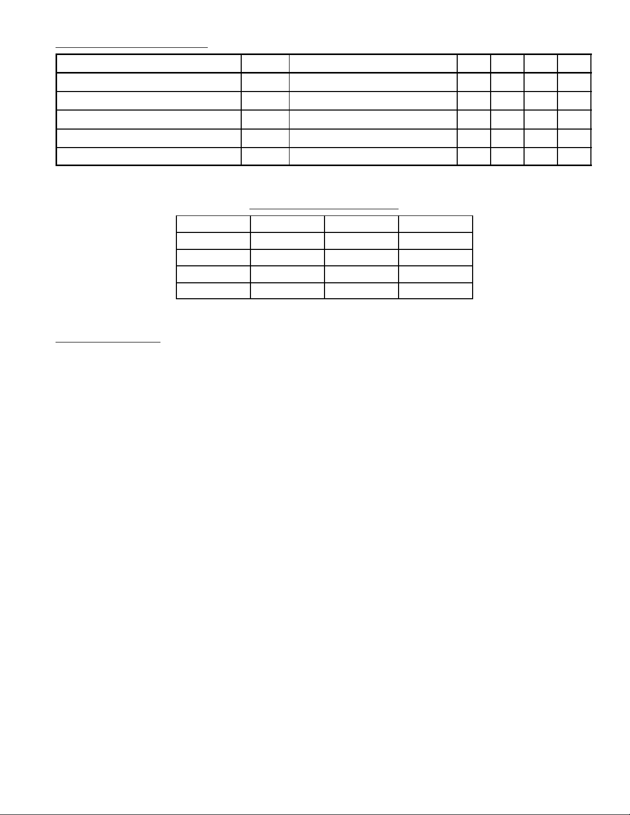
Pin Connection Diagram
(Front View)
V
10
9
VZ (2)
VCC (2)
8
VCC (1)
7
Input (Reverse)
6
Input (Forward)
5
V
4
VZ (1)
3
V
2
GND
1
OUT
REG
OUT
(2)
(1)
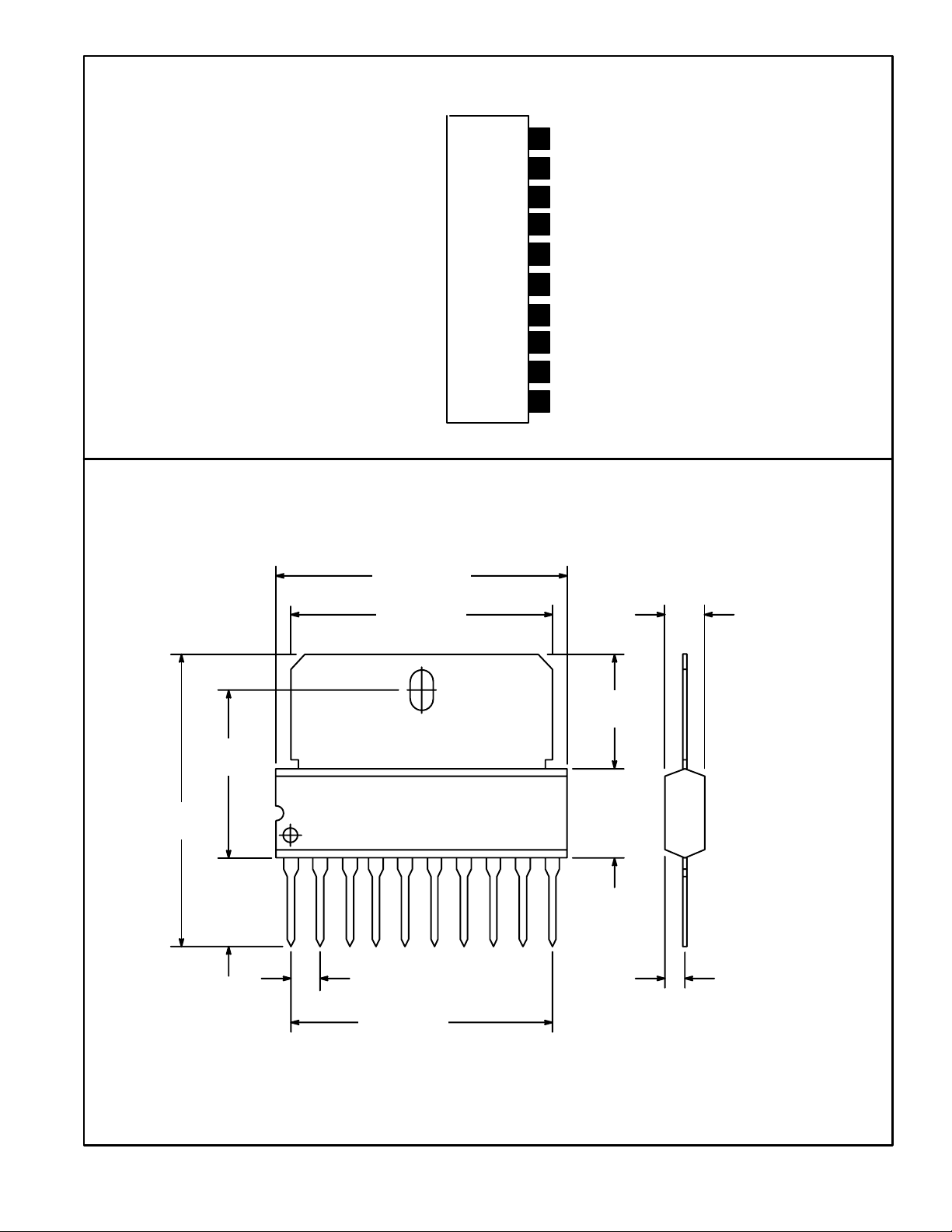
1.063
(27.0)
.700
(17.78)
.251
(6.4)
1.043 (26.5)
.984 (25.0)
.141 (3.6)
.409
(10.4)
.330
(8.38)
110
.100 (2.54)
.070 (1.78)
.897 (22.8)
 Loading...