

NTE NTE1710 Datasheet
NTE1710
Integrated Circuit
Record/Playback Circuit for VCR
Description:
The NTE1710 is an integrated circuit in a 22–Lead DIP type package designed for tape recorder and
VCR audio recording and playback. This device has built–in electronic switches for recording and
playback which include the ones for a noise reduction circuit.
Features:
D Electronic Switches for REC/PLAY Operation Included (Noise–Reduction Switches also Possible)
D Low Noise (Noise Voltage Referred to Input = 0.95µV P.B., Rg = 2.2kΩ, 20Hz to 20kHz)
D Almost All Functions Necessary for REC/PLAY operation and AGC Circuit Included
D Low Current Consumption
D Muting Possible Externally
Absolute Maximum Ratings: (TA = +25°C unless otherwiser specified)
Supply Voltage, V
Power Dissipation, P
CC
D
Operating Temperature Range, T
Storage Temperature Range, T
stg
opr
–20° to +70°C. . . . . . . . . . . . . . . . . . . . . . . . . . . . . . . . . . . . . . . . .
–55° to +150°C. . . . . . . . . . . . . . . . . . . . . . . . . . . . . . . . . . . . . . . . . .
14.4V. . . . . . . . . . . . . . . . . . . . . . . . . . . . . . . . . . . . . . . . . . . . . . . . . . . . . . . . . . . . . .
700mW. . . . . . . . . . . . . . . . . . . . . . . . . . . . . . . . . . . . . . . . . . . . . . . . . . . . . . . . . . .
Electrical Characteristics: (VCC = 9V, TA = +25°C unless otherwise specified)
Parameter Symbol Test Conditions Min Typ Max Unit
Closed Loop Output Voltage
On Playback Mode
On Record Mode V
Total Harmonic Distortion THD P.B., Line Out, Vi = 1kHz, 1.58mV – 0.06 0.1 %
Maximum Output Voltage
Line Output
Recording Output Rec., f = 1kHz, THD = 1% 1.7 2.2 – V
Output Noise Voltage
Playback Head Input
Record MIC Input Rec., Rg = 2.2kΩ, f = 20Hz to 20kHz – 1.5 2.5 mV
Record Line Input Rec., Rg = 0, f = 20Hz to 20kHz – 0.14 0.3 mV
Playback Head Input P.B., Rg = 0, f = 20Hz to 20kHz – 1.7 3.0 mV
V
O(PB)
O(REC)
V
O(max)
V
no
P.B., Line Out, Vi = 1kHz, 0.158mV 420 500 594 mV
Rec., Rec Out, AGC: OFF, Vi = 1kHz, 0.315mV 315 445 628 mV
P.B., f = 1kHz, THD = 1% 1.7 2.2 – V
P.B., Rg = 2.2kΩ, f = 20Hz to 20kHz – 3.0 5.5 mV
rms
rms
Note 1. A capacitor of 10µF or over must be used between Pin11 and GND for the purpose of
preventing the AGC circuit oscillation when it is actually used.
Electrical Characteristics (Cont’d): (VCC = 9V, TA = +25°C unless otherwise specified)
Parameter Symbol Test Conditions Min Typ Max Unit
AGC Output Voltage V
AGC Distortion THD–A – 0.15 0.3 %
R/P–SW Leakage Voltage V
Muting ON Leakage Voltage V
Total Supply Current I
Mode handling Voltage
Playback Mode
Record Mode V
Muting Holding Voltage
OFF Mode
ON Mode V
O(AGC)
Leak(P/R)
Leak(Mute)
tot
V
18–P
18–R
V
17–OFF
17–ON
Rec., AGC: ON, Rec. Out, Vi = 1kHz, 0.315mV 315 445 570 mV
Rec., AGC: ON, Rec. Out, Vi = 1kHz, 31.5mV 700 825 950 mV
Rec., Rec Out, Vi (PB Input) 1kHz 16mV,
Rec. Input Shorted
P.B., Line Out, Vi (MIC Input) 1kHz 31.5mV,
P.B. Input Shorted
Rec., Rec Out, Vi (MIC Input) 1kHz 0.5mV,
P.B. Input Shorted
P.B., Mute: OFF 5.5 9.0 12.5 mA
– 1.0 6.0 mV
– 1.8 10 mV
– 50 100 µV
0 – 0.7 V
3.5 – 7.0 V
0 – 0.9 V
2.4 – 4.0 V
Note 1. A capacitor of 10µF or over must be used between Pin11 and GND for the purpose of
preventing the AGC circuit oscillation when it is actually used.
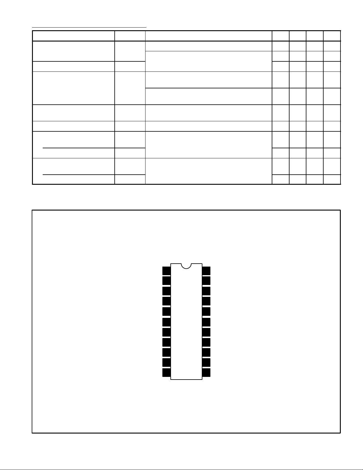
Pin Connection Diagram
EQ Input
EQ Neg Feedback
EQ Output
Buffer Input (Playback)
Buffer Feedback (Record)
Buffer Output
Line Input (Record)
Line Input (Playback)
Line Output
GND
AGC Control
1
2
3
4
5
6
7
8
22
21
20
19
18
17
16
15
10 13
11 12
MIC Input
MIC Neg Feedback
MIC Output
AGC Input
Record/Playback Switch
Muting Switch
Rec Input
Rec Neg Feedback
Rec Output9 14
Reference Voltage
V
CC
 Loading...