

NTE1700
Integrated Circuit
2, 4, & 6 Hour Auto Discriminator for VCR
Description:
The NTE1700 is an integrated circuit in an 18–Lead DIP type package designed for 2Hr/4Hr/6Hr automatic selection in video cassette recorders.
Features:
D The Functions Consist of:
Capstan FG Frequency Divider
Monostable Mulitvibrator
Sample & Hold Circuit
D Supply Voltage Either 9V or 12V
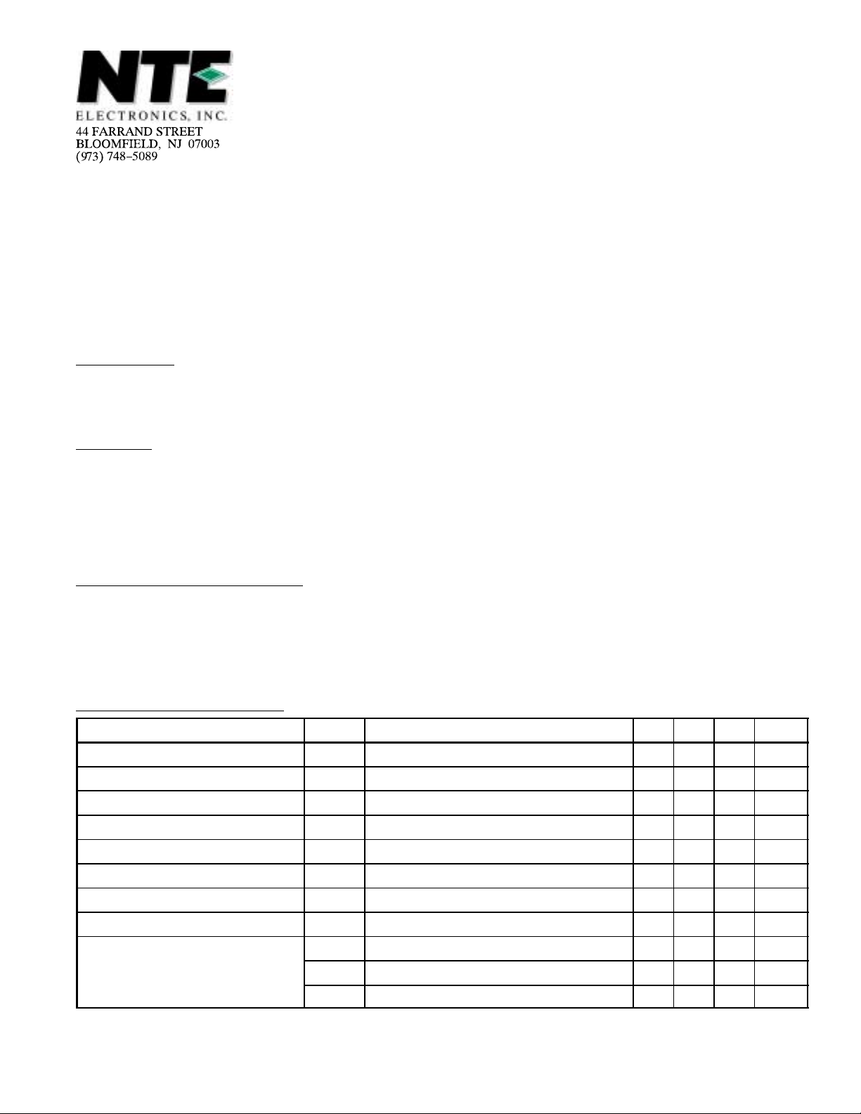
Absolute Maximum Ratings: (TA = +25°C unless otherwise specified)
Supply Voltage, V
Power Dissipation (TA = +70°C), P
CC
D
Operating Ambient Temperature Range, T
Storage Temperature Range, T
stg
opr
–20° to +70°C. . . . . . . . . . . . . . . . . . . . . . . . . . . . . . . . . .
–40° to +150°C. . . . . . . . . . . . . . . . . . . . . . . . . . . . . . . . . . . . . . . . . .
13V. . . . . . . . . . . . . . . . . . . . . . . . . . . . . . . . . . . . . . . . . . . . . . . . . . . . . . . . . . . . . . . .
500mW. . . . . . . . . . . . . . . . . . . . . . . . . . . . . . . . . . . . . . . . . . . . . . .
Electrical Characteristics: (VCC = V
Parameter Symbol Test Conditions Min Typ Max Unit
Supply Current I
Input Blind Level V
Playback Control Amp Sensitivity S
X9 Select Sensitivity S
X2 Select Sensitivity S
1/2 Slow Select Sensitivity S
Triangular Wave Reference Voltage V
Pause “L” Voltage V
S/H Output Voltage V
OL11
V
O(C–11)
V
OH11
14
2
2
3
4–1
4–2
7
11
Note 1. Operating Supply Voltage: V
= 12V, TA = +25°C ±2°C unless otherwise specified)
14–1
24 – 40 mA
– – 150 mV
350 – – mV
SW. A to 1 3.3 – – V
SW. A to 2 5.5 – – V
SW. A to 3 – – 1.45 V
V
= 0, from Pin7 30kΩ to GND 2.9 – 3.6 V
6–1
V
= 7V, V
5–1
SW. to 1 1.85 – 2.15 V
SW. to 3 3.25 – 3.80 V
SW. to 2 6.25 – 7.15 V
CC(opr)
= 8.5V to 12.5V
= 5.5V 3.3 – 4.1 V
10–1
P–P
P–P
Electrical Characteristics (Cont’d): (VCC = V
Parameter Symbol Test Conditions Min Typ Max Unit
= 12V, TA = +25°C ±2°C unless otherwise specified)
14–1
2H Select Sensitivity S
4H Select Sensitivity S
6H Select Sensitivity S
Record Select Sensitivity S
A Output “H” V oltage V
A Output “L” V oltage V
B Output “H” V oltage V
B Output “L” V oltage V
Muting Output “H” Voltage V
Muting Output “L” Voltage V
A Schmitting Output “H” Voltage V
A Schmitting Output “L” Voltage V
B Schmitting Output “H” Voltage V
B Schmitting Output “L” Voltage V
12–1
12–2
12–3
13
15HI15–1
15LI15–1
16HI16–1
16LI16–1
18H
18L
OH(A)
OL(A)
OH(B)
OL(B)
Note 1. Operating Supply Voltage: V
V
13–1
V
13–1
V
13–1
CC(opr)
= 3.3V, SW. to 1 5.5 – – V
= 3.3V, SW. to 2 2.4 – 3.8 V
= 3.3V, SW. to 3 – – 1.45 V
3.3 – – V
= –3mA, V
= 5mA, V
= –3mA, V
= 5mA, V
12–1
12–1
12–1
12–1
= 5.5V, V
= 5.5V, V
= 1.45V, V
= 1.45V, V
= 3.3V 10 – – V
13–1
= 3.3V – – 0.55 V
13–1
= 3.3V 10 – – V
13–1
= 3.3V – – 0.55 V
13–1
5.2 – – V
– – 0.2 V
5.6 – 6.5 V
2.8 – 3.4 V
4.15 – 4.8 V
2.8 – 3.4 V
= 8.5V to 12.5V
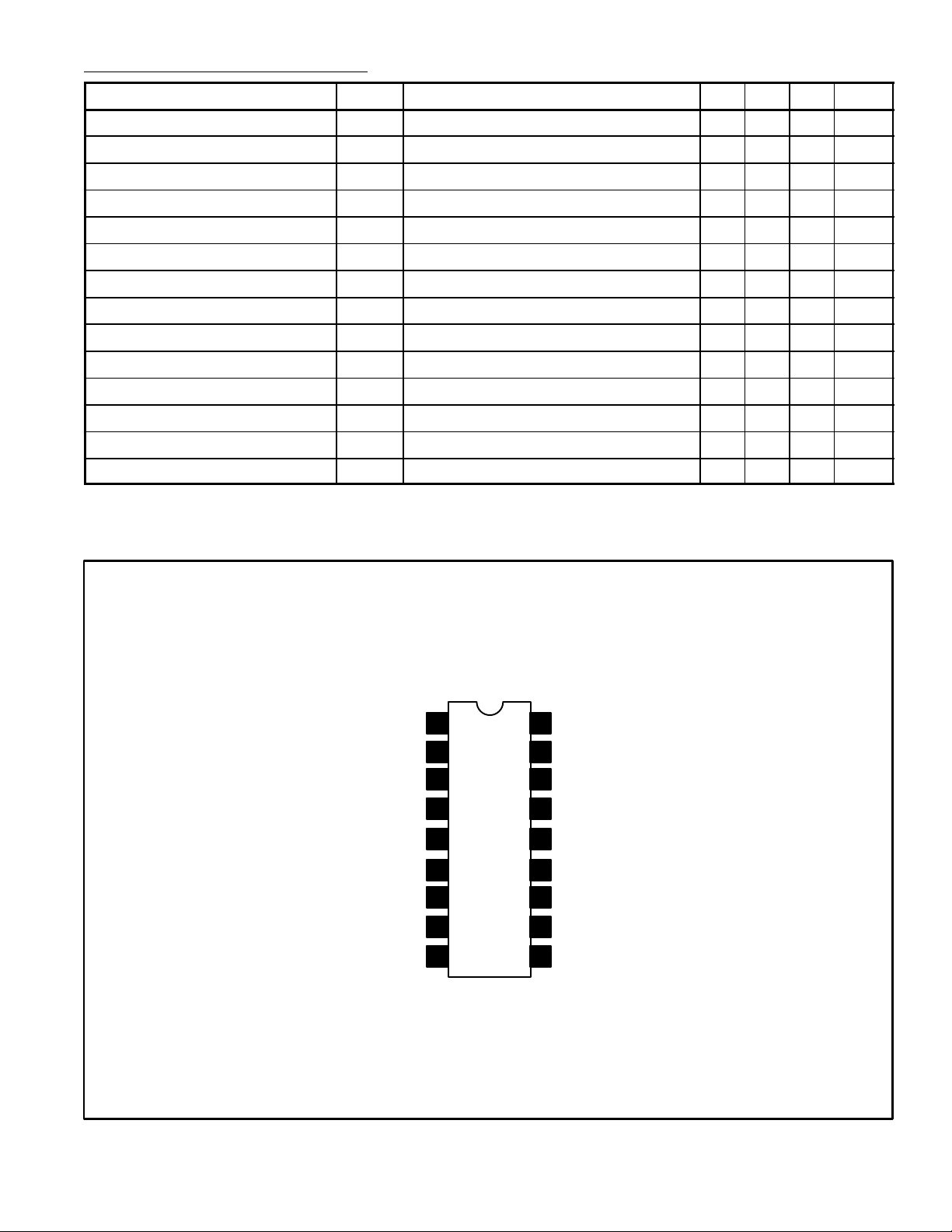
Pin Connection Diagram
GND
PB Control Signal Input
X9 Select
X2, Normal, 1/2 Select
1
2
3
4
5Sample Pulse
6Triangle Wave C
7Triangle Wave R
8Sample Hold
18
17
16
15
14
13
12
11
9Signal Detect 10
Muting Output
Muting C, R
B Output
A Output
V
CC
Rec/PB Select
2/4/6 Hour Select
L.P.F.
Pause L
 Loading...