


NTE1687
Linear Integrated Circuit
Dual, 2.5W (7.8W BTL) Audio Amp
Description:
The NTE1687 is a high performance stereo power amplifier in an 11–Lead SIP type package designed to deliver 1W/Ch into 4Ω or 2W bridged monaural into 8Ω. It is ideal for sensitive AM radio
applications, exhibiting lower wideband noise, lower distortion, and less AM radiation than conventional designs.
Features:
D Low AM Radiation
D Low Noise
D 3V, 4Ω, Stereo PO = 250mW
D Wide Supply Operation: 3V to 15V
D Low Distortion
D PO = 9W Bridged
Applications:
D Compact AM/FM Radios
D Stereo Tape Recorders and Players
D High Power Portable Stereos
Absolute Maximum Ratings:
Supply Voltage, V
Junction Temperature, T
Operating Temperature Range (Note 1), T
Storage Temperature Range, T
S
J
opr
stg
Lead Temperature (During Soldering, 10 sec), T
0°C to +70°C. . . . . . . . . . . . . . . . . . . . . . . . . . . . . . . . . . .
–65°C to +150°C. . . . . . . . . . . . . . . . . . . . . . . . . . . . . . . . . . . . . . . .
L
18V. . . . . . . . . . . . . . . . . . . . . . . . . . . . . . . . . . . . . . . . . . . . . . . . . . . . . . . . . . . . . . . . .
+150°C. . . . . . . . . . . . . . . . . . . . . . . . . . . . . . . . . . . . . . . . . . . . . . . . . . . . . . . . .
+260°C. . . . . . . . . . . . . . . . . . . . . . . . . . . . . . . . . . . .
Note 1. For operation at ambient temperature greater than +25°C, the NTE1687 must be derated
based on a maximum +150°C junction temperature using a thermal resistance which depends upon mounting techniques,
Electrical Characteristics: (TA = 25°C, AV = 200 (46dB), T
= 25°C, VS = 12V, RL = 8Ω,
TAB
unless otherwise specified)
Parameter Test Conditions Min Typ Max Unit
Supply Current PO = 0W, Dual Mode – 25 40 mA
Operating Supply Voltage 3 – 15 V
Output Power THD = 10%,
f = 1kHz
Distortion f = 1kHz
Power Supply Rejection Ratio
(PSRR)
Channel Separation CBY = 100µF, f = 1kHz, CIN = 0.1µF, Output Referred –50 –64 – dB
Noise
DC Output Level 5.6 6 6.4 V
Input Impedance 50 100 350 kΩ
Input Offset Voltage – 5 – mV
Voltage Difference between
Outputs
Input Bias Current – 120 – nA
CBY = 100µF, f = 1kHz, CIN = 0.1µF, Output Referred,
V
RIPPLE
Equivalent
Input Noise
R = 0
RS = 0
VS = 12V, RL = 8Ω Dual Mode 2.0 2.5 – W/Ch
VS = 12V, RL = 8Ω Bridge Mode 7.2 9.0 – W
VS = 9V, RL = 4Ω Bridge Mode – 7.8 – W
VS = 9V, RL = 4Ω Dual Mode – 2.5 – W/Ch
PO = 50mW – 0.09 –
PO = 0.5W – 0.11 –
PO = 1W – 0.14 –
–40 –54 – dB
= 250mV
CIN = 0.1µF, BW = 20 – 20kHz – 1.4 – µV
CCIR/ARM – 1.4 –
Wideband – 2.0 –
– 10 20 mV
%
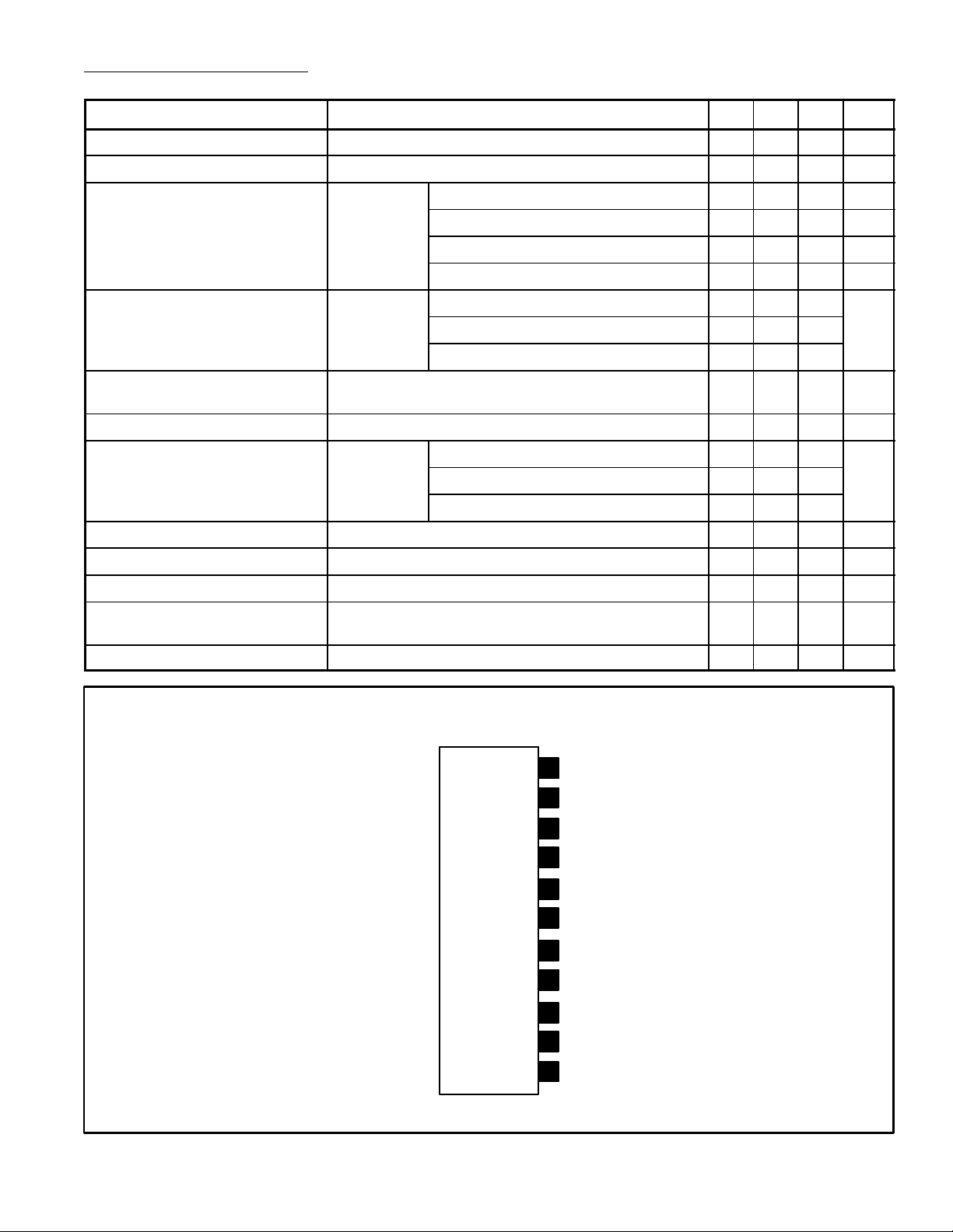
Pin Connection Diagram
(Front View)
11
10
9
8
7
6
5
4
3
2
1
Bypass
Output 1
Bootstrap 1
(–) Input 1
(+) Input 1
GND
(+) Input 2
(–) Input 2
Bootstrap 2
Output 2
(+) V
S
 Loading...