

NTE1684
Integrated Circuit
TV Vertical Deflection Output Circuit
Description:
The NTE1684 is an integrated circuit in a 7–Lead SIP type package designed for use in TV vertical
deflection output circuits.
Features:
D High Breakdown Voltage
D Low Power Consumption
Absolute Maximum Ratings:
Supply Voltage, V
Circuit Voltage, V
Circuit Voltage, V
Circuit Voltage, V
Supply Current, I
Circuit Current, I
Power Dissipation, P
CC
3–1
4–1
5–1
CC
, I
. . . . . . . . . . . . . . . . . . . . . . . . . . . . . . . . . . . . . . . . . . . . . . . .
2
6
D
(TA = +25°C unless otherwise specified)
Operating Ambient Temperature Range, T
Storage Temperature Range, T
stg
Thermal Resistance, Junction–to–Case, R
Electrical Characteristics:
Parameter Symbol Test Conditions Min Typ Max Unit
Deflection Current I
Deflection Current Linearity ∆I
Deflection Current Change with
Ambient Temperature
(TA = +25°C unless otherwise specified)
y(P–P)
y(+)
∆I
y(–)
∆Iy/TATA = –20° to +70°C –1.5 – +1.5 %
opr
thJC
0 to 60V. . . . . . . . . . . . . . . . . . . . . . . . . . . . . . . . . . . . . . . . . . . . . . . . . . . . . . . . . . . .
–1V to 6V. . . . . . . . . . . . . . . . . . . . . . . . . . . . . . . . . . . . . . . . . . . . . . . . . . . . . . . . . . .
–1V to 3V. . . . . . . . . . . . . . . . . . . . . . . . . . . . . . . . . . . . . . . . . . . . . . . . . . . . . . . . . . .
300mA. . . . . . . . . . . . . . . . . . . . . . . . . . . . . . . . . . . . . . . . . . . . . . . . . . . . . . . . . . . . . .
–1300 to 1300mA
–20° to +70°C. . . . . . . . . . . . . . . . . . . . . . . . . . . . . . . . . .
–55° to +150°C. . . . . . . . . . . . . . . . . . . . . . . . . . . . . . . . . . . . . . . . . .
4°C/W. . . . . . . . . . . . . . . . . . . . . . . . . . . . . . . . . . . . . . .
1280 1380 1480 mA
46 – 140 mA
42 – 126 mA
30V. . . . . . . . . . . . . . . . . . . . . . . . . . . . . . . . . . . . . . . . . . . . . . . . . . . . . . . . . . . . . . . .
O–P
6W. . . . . . . . . . . . . . . . . . . . . . . . . . . . . . . . . . . . . . . . . . . . . . . . . . . . . . . . . . . . . .
P–P
P–P
P–P
Center Voltage V
Flyback Pulse Amplitude V
Static Circuit Current I
MID
(FBP)
CQ
V
3–1
= 24V, V
= 24V, V
7–1
13.2 13.8 14.4 V
47 – – V
= 0 8 14 24 mA
5–1
Electrical Characteristics (Cont’d): (TA = +25°C unless otherwise specified)
Parameter Symbol Test Conditions Min Typ Max Unit
Output Transistor Saturation Voltage V
Q21 Saturation Voltage V
V
3–2
V
2–1
6–1
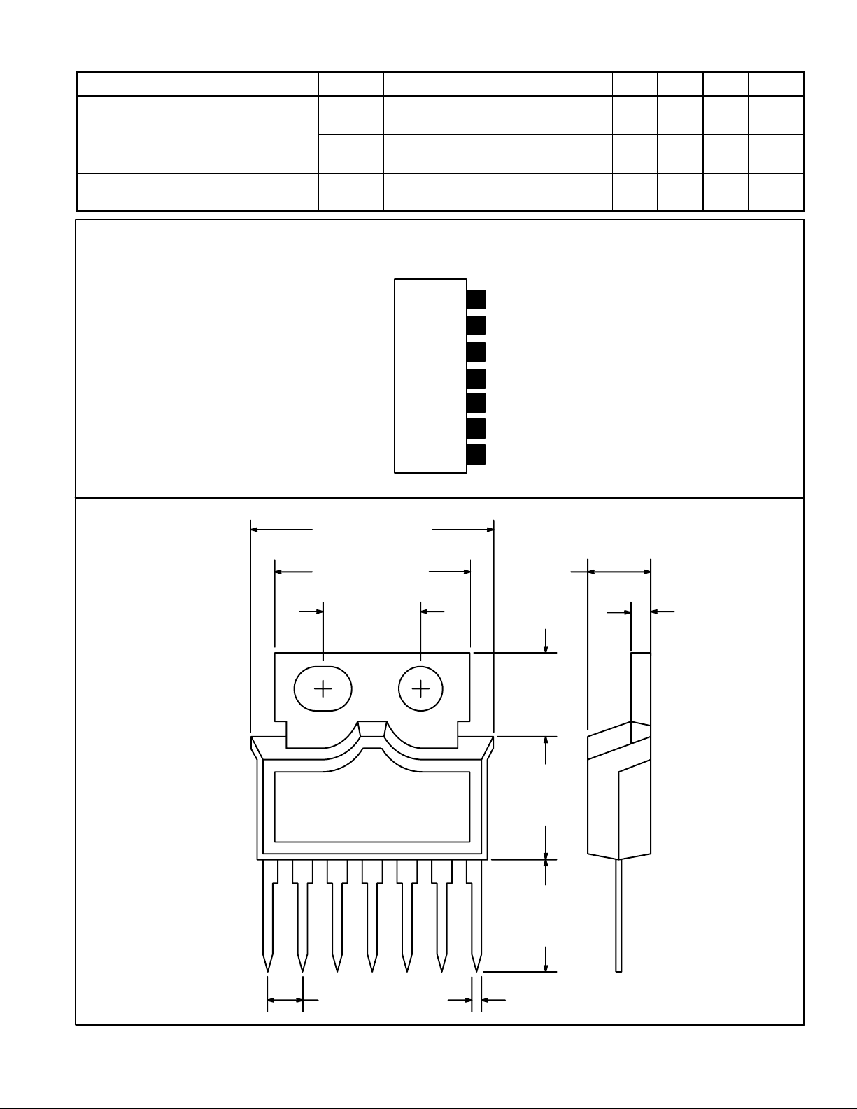
Pin Connection Diagram
= V
3–1
= 0.3V, V
V
4–1
V
= V
3–1
= 1.3V, V
V
4–1
V
= 24V, Pin7–6 = 1.2kΩ,
7–1
= 0, V
V
5–1
(Front View)
= 24V, Pin2–1 = 56Ω,
7–1
= 24V, Pin2–3 = 56Ω,
7–1
4–1
= 0
5–1
= 0
5–1
= 2V
V
7
CC
Pulse Amp Output
6
Trigger Pulse Input
5
4
Input
3
Supply Voltage for Output
Output
2
1
GND
– 2.6 3.6 V
– 0.4 1.0 V
– – 0.5 V
.697 (17.2)
.602 (15.3)
.300 (7.6)
17
.138
(3.5)
.047
(1.2)
.233
(5.9)
.323
(8.2)
.308
(7.8)
.100 (2.54) .024 (0.6)
 Loading...