

NTE1674
Integrated Circuit
TV Vertical Deflection Output Circuit
Description:
The NTE1674 is an integrated circuit in a 9–Lead SIP type package designed for use as a TV vertical
deflection output circuit. When used in combination with a deflection signal processing IC, this device
can facilitate a vertical output circuit design.
Features:
D Low Power Consumption
D Direct Deflection Coil Driving Capability
D High Breakdown Voltage
Absolute Maximum Ratings: (TA = +25°C unless otherwise specified)
Supply Voltage, V
Circuit Voltage, V
Circuit Voltage, V
Circuit Voltage, V
Supply Current, I
Circuit Current, I
Circuit Current, I
Power Dissipation, P
CC
4–1
6–1
7–1
CC
. . . . . . . . . . . . . . . . . . . . . . . . . . . . . . . . . . . . . . . . . . . . . . . . . .
2
. . . . . . . . . . . . . . . . . . . . . . . . . . . . . . . . . . . . . . . . . . . . . . . . . .
8
D
Operating Ambient Temperature Range, T
Storage Temperature Range, T
stg
Thermal Resistance, Junction–to–Case, R
opr
thJC
–1000 to +1000mA
–1000 to +1000mA
–20° to +70°C. . . . . . . . . . . . . . . . . . . . . . . . . . . . . . . . . .
–55° to +150°C. . . . . . . . . . . . . . . . . . . . . . . . . . . . . . . . . . . . . . . . . .
27.6V. . . . . . . . . . . . . . . . . . . . . . . . . . . . . . . . . . . . . . . . . . . . . . . . . . . . . . . . . . . . . .
0 to 60V. . . . . . . . . . . . . . . . . . . . . . . . . . . . . . . . . . . . . . . . . . . . . . . . . . . . . . . . . . . .
0 to 2.5V. . . . . . . . . . . . . . . . . . . . . . . . . . . . . . . . . . . . . . . . . . . . . . . . . . . . . . . . . . .
0 to 1.3V. . . . . . . . . . . . . . . . . . . . . . . . . . . . . . . . . . . . . . . . . . . . . . . . . . . . . . . . . . .
250mA. . . . . . . . . . . . . . . . . . . . . . . . . . . . . . . . . . . . . . . . . . . . . . . . . . . . . . . . . . . . . .
O–P
O–P
6.66W. . . . . . . . . . . . . . . . . . . . . . . . . . . . . . . . . . . . . . . . . . . . . . . . . . . . . . . . . . . .
12°C/W. . . . . . . . . . . . . . . . . . . . . . . . . . . . . . . . . . . . . .
Note 1. and are flow–in and flow–out currents to/from the circuit respectively.
Electrical Characteristics: (TA = +25°C unless otherwise specified)
Parameter Symbol Test Conditions Min Typ Max Unit
Deflection Current I
Deflection Current Linearity DI
Deflection Current Change with
Ambient Temperature
y(P–P)
DI
DIy/T
y(+)
y(–)
TA = –20° to +70°C –1.5 – +1.5 %
A
860 930 1000 mA
25 – 75 mA
22 – 85 mA
P–P
P–P
P–P
Electrical Characteristics (Cont’d): (TA = +25°C unless otherwise specified)
Parameter Symbol Test Conditions Min Typ Max Unit
Center Voltage V
Flyback Pulse Amplitude V
Static Circuit Current I
Output Transistor Saturation Voltage V
Q21 Saturation Voltage V
MID
(FBP)
V
CQ
4–2
V
2–1
8–1
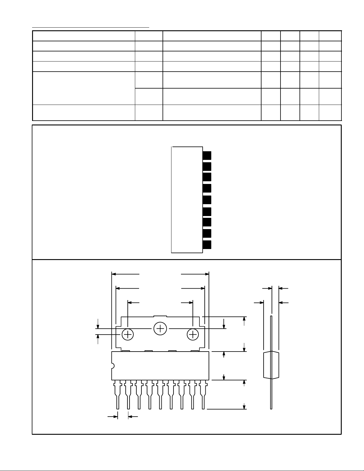
Pin Connection Diagram
= 24V, V
4–1
V
= V
4–1
V
= 0.3V, V
6–1
V
= V
4–1
V
= 1.3V, V
6–1
V
= 24V, Pin9 – 8 = 1.2kΩ,
9–1
V
= 0V
7–1
(Front View)
= 24V, Pin2 – 1 = 56Ω,
9–1
= 24V, Pin2 – 4 = 56Ω,
9–1
= 24V, V
9–1
= 0V
7–1
= 0V
7–1
9
V
CC
8
Pulse Amp Output
Trigger Pulse Input
7
6
Input
Drive Transistor Collector
5
Supply Voltage for Output
4
= 0V 7 13 22 mA
7–1
12.1 12.6 13.1 V
47 – – V
– 2.7 3.7 V
– 0.6 1.0 V
– – 0.5 V
.059
(1.5)
N.C.
3
Output
2
GND
1
.890 (22.6)
.728 (18.5)
.591 (15.0)
.067 (1.72)
.150 (3.8)
.328
.229
(8.33)
(5.82)
.250
(6.35)
19
.281
(7.14)
.100 (2.54)
 Loading...