

NTE NTE1639 Datasheet
NTE1639
Integrated Circuit
CMOS Clock Generator/Driver for BBDs
Description:
The NTE1639 is a CMOS LSI Clock Generator ina 8–Lead DIP type package capable of generating
two phase clock signals of low output impedance for use as a BBD driver. The built–in V
supply circuit provides the proper voltages needed for driving BBDs such as the NTE1641.
Features:
D BBD Direct Driving Capability of up to two BBD’s
D Self and Separate Oscillations.
D Two Phase Clock Output (Duty: 1/2)
D Built–in V
Voltage Generator for Driving the NTE1641 BBD.
GG
D Single Power Supply: –8V to –16V.
Applications:
D BBD Clock Generator/Driver.
GG
power
Absolute Maximum Ratings:
Drain Supply Voltage, V
DD
Input/Output Pin Voltage, V
Power Dissipation, P
D
(TA = +25°C unless otherwise specified)
I, VO
Operating Ambient Temperature Range, T
Storage Temperature Range, T
stg
Recommended Operating Conditions:
Item
Drain Supply Voltage V
Symbol Condition Min Typ Max Unit
DD
GND = 0V –8 –15 –16 V
VDD –0.3V to +0.3V. . . . . . . . . . . . . . . . . . . . . . . . . . . . . . . . . . . . . . . .
opr
(TA = +25°C unless otherwise specified)
–18V to +0.3V. . . . . . . . . . . . . . . . . . . . . . . . . . . . . . . . . . . . . . . . . . . . . . . . . .
200mW. . . . . . . . . . . . . . . . . . . . . . . . . . . . . . . . . . . . . . . . . . . . . . . . . . . . . . . . . .
–10° to +70°C. . . . . . . . . . . . . . . . . . . . . . . . . . . . . . . . . .
–30° to +125°C. . . . . . . . . . . . . . . . . . . . . . . . . . . . . . . . . . . . . . . . . .
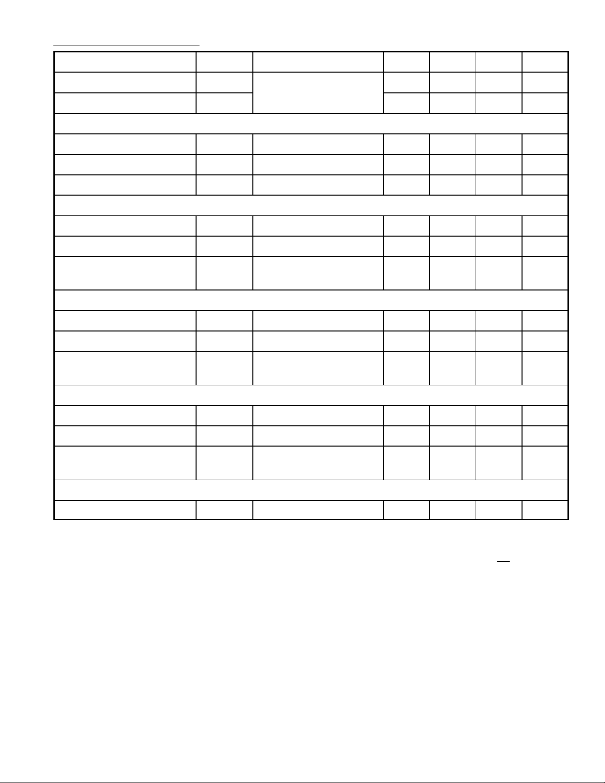
Electrical Characteristics: (TA = +25°C, VDD = –15V, GND = 0V unless otherwise specified)
Parameter
Symbol Test Condition Min Typ Max Unit
Input Drain Current I
Total Power Dissipation P
OX1 Input Pin
Voltage “H” Level V
Voltage “L” Level V
Input Leakage Current I
Leak
OX2 Output Pin
Output Current “H” Level I
Output Current “L” Level I
Output Leakage Current I
OH(1)
OL(1)
LOL(1)
OX3 Output pin
Output Current “H” Level I
Output Current “L” Level I
OH(2)
OL(2)
DD
tot
IH
IL
No load
No load
Clock Output 40kH
Z
– 3 – mA
– 45 – mW
0 – –1 V
VDD+1 – V
DD
V
VI = 0V to –15V – – 30 µA
VO = –1V 0.6 – – mA
VO = –14V 0.5 – – mA
VO = V
DD
VO = GND
–
–
–
–
30
30
µA
µA
VO = –1V 1.5 – – mA
VO = –14V 2 – – mA
Output Leakage Current I
LOL(2)
VO = V
DD
VO = GND
CP1, CP2 output pin
Output Current “H” Level I
Output Current “L” Level I
Output Leakage Current I
OH(3)
OL(3)
LOL(3)
VO = –1V 10 – – mA
VO = –14V 10 – – mA
VO = V
DD
VO = GND
VGG OUT output pin (Note 1)
Output Voltage V
GG(Out)
Note 1. This pin generates the VGG voltage for a BBD manufac-
tured by NTE. So therefore, it might not be applicable for
other devices. In any case, the V
GG(OUT)
changes by the
following formula depending on the value of VDD.
–
–
–
–
–
–
–
–
30
30
30
30
–14 V
14
V
GG(OUT)
≅
15
V
µA
µA
µA
µA
DD
 Loading...