

NTE NTE1634 Datasheet
NTE1634
Integrated Circuit
Dual Preamp w/ALC
Description:
The NTE1634 is a monolithic integrated circuit in a 14–Lead DIP type package consisting of a dual
equalizer ampli fier w i th autom atic l evel c ontr ol ( ALC) a nd is suitable f or s ter eo r adio c assette applications.
Features:
D Dual Equalizer Amplifier with Built–In ALC Circuit.
D Recording Amp Available Because of High Gain Characteristic (Variable Monitor Possible).
D Good Channel Separation (Sep = 50dB Typ)
D Capable of Direct Meter Driving and ALS Transistor.
D Good ALC Response Balance Between Channels.
D Wider Operating Supply Voltage Range (4V to 13V)
Absolute Maximum Ratings: (TA = +25°C unles otherwise specified)
Supply Voltage, V
CC
Power Dissipation, PD 600mW. . . . . . . . . . . . . . . . . . . . . . . . . . . . . . . . . . . . . . . . . . . . . . . . . . . . . . . . . . .
Operating Temperature Range, T
Storage Temperature Range, T
stg
opr
–20° to +70°C. . . . . . . . . . . . . . . . . . . . . . . . . . . . . . . . . . . . . . . . .
–40° to +125°C. . . . . . . . . . . . . . . . . . . . . . . . . . . . . . . . . . . . . . . . . .
ALC TR Maximum Current 3.5mA. . . . . . . . . . . . . . . . . . . . . . . . . . . . . . . . . . . . . . . . . . . . . . . . . . . . . . . .
14V. . . . . . . . . . . . . . . . . . . . . . . . . . . . . . . . . . . . . . . . . . . . . . . . . . . . . . . . . . . . . . . .
Electrical Characteristic: (TA = +25°C, VCC = 5V, RL = 10kΩ: Playback, RL = 680Ω: Recording
unless otherwise specified)
Parameter Symbol Test Conditions Min Typ Max Unit
Circuit Current I
Voltage Gain (Open Loop) A
Voltage Gain (Closed Loop) A
Output Voltage V
Total Harmonic Distortion THD VO = 0.5V, Play – 0.1 1.0 %
Input Resistance R
Equivalent Input Noise Voltage V
Cross Talk CT Rg = 2.2KΩ 40 50 – dB
ALC Range Vi = –60dBm, Record 35 45 – dB
ALC Balance Vi = –20dBm, Record – 0 2.0 dB
ALC Distortion Vi = –20dBm, Record – 0.5 2.0 %
A
CC
VO
V1
V2
O
NI
Vi = 0 – 4.5 10 mA
– 85 – dB
Play – 40 – dB
Record – 58 – dB
THD = 1%, Play 0.9 1.2 – V
i
BW(–3dB)=20Hz to 20kHz – 1.0 2.0 µV
21 30 – kΩ
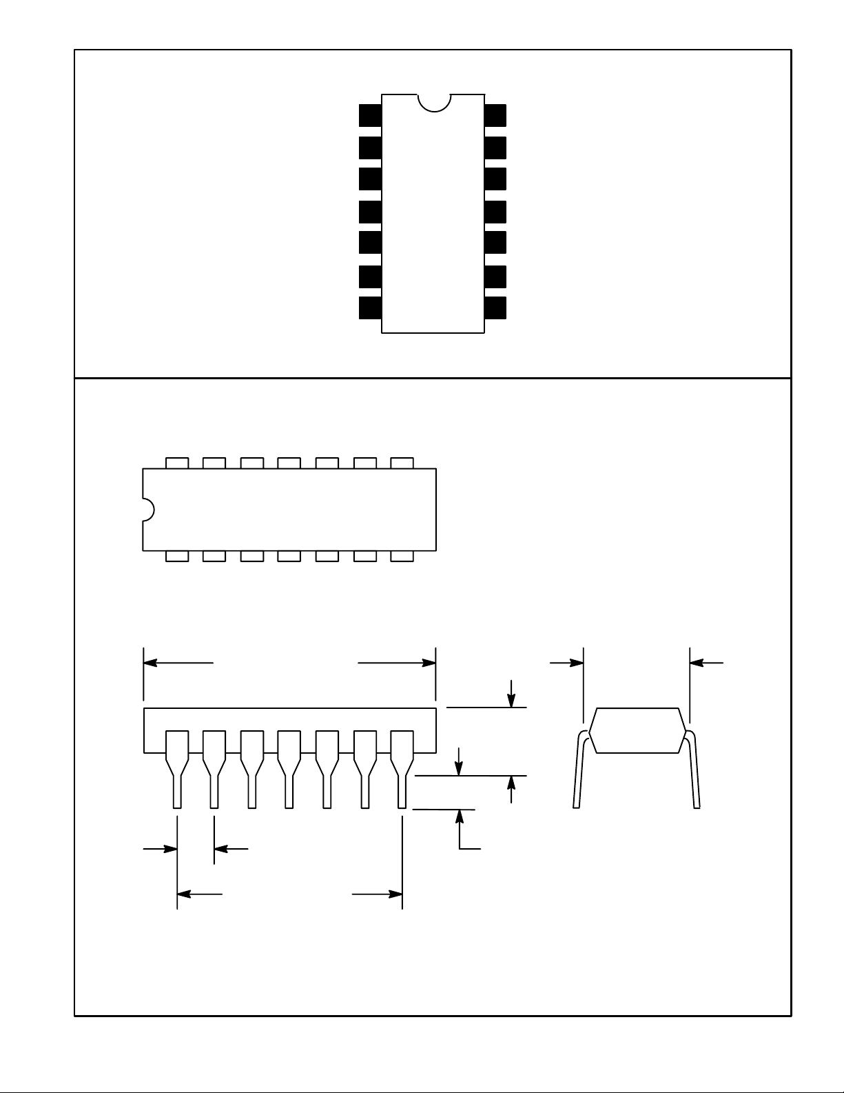
Pin Connection Diagram
GND
Output 1
PC 1
NF 1
1
2
3
4
5Input 1
6ALC Output 1
7ALC Input
14 8
14
V
CC
Output 2
13
12
PC 2
11
NF 2
10 Input 2
9 ALC Output 2
8 DC
17
.785 (19.95) Max
.300 (7.62)
.200 (5.08)
Max
.100 (2.45) .099 (2.5) Min
.600 (15.24)
 Loading...