


NTE1570 (NPN Tuner) & NTE1572 (FET Tuner)
Integrated Circuit
TV Video IF, Sound IF
Functions:
PIF
D Three Controlled IF Amplifier Stages
D Video Demodulator Controlled by Picture Carrier
D Black Noise and White Noise Inverter
D Peak AGC
D DC Amplifier for RF AGC Out
Features:
D PIF, SIF, ATT Audio Driver
D 2 Chip Color TV System is Possible with NTE1547
SIF
D Three Differential IF Amplifier Stages
D Phase Detector
D DC Controlled Attenuator
D Audio Amplifier Stage with NFB Terminal
PIF
D High Gain, Wide Band IF Amplifier
D AGC Characteristics with Excellent Stability
SIF
D Excellent Limiter Charactristics
D Excellent Attenuato Characteristics
D Excellent DG/DP Characteristics
D Excellent S/N Chracteristics due to Delayed 3
Stage AGC Action
D Negative Video Output Signal
D Switch Off the Video Part with VTR Switch
Absolute Maximum Ratings: (TA = +25°C unless otherwise specified)
Supply Voltage, V
Pin11 Open Voltage, V
Video DC Output Current, I
Audio DC Output Current, I
Pin2 Voltage, V
Power Dissipation, P
CC
11
15
3
2
D
Derate Above 25°C 12.8mW/°C. . . . . . . . . . . . . . . . . . . . . . . . . . . . . . . . . . . . . . . . . . . . . . . . . . . .
Operating Temperature Range, T
Storage Temperature range, T
opr
stg
15V. . . . . . . . . . . . . . . . . . . . . . . . . . . . . . . . . . . . . . . . . . . . . . . . . . . . . . . . . . . . . . . .
15V. . . . . . . . . . . . . . . . . . . . . . . . . . . . . . . . . . . . . . . . . . . . . . . . . . . . . . . . . . . .
6mA. . . . . . . . . . . . . . . . . . . . . . . . . . . . . . . . . . . . . . . . . . . . . . . . . . . . . . .
3mA. . . . . . . . . . . . . . . . . . . . . . . . . . . . . . . . . . . . . . . . . . . . . . . . . . . . . . . .
15V. . . . . . . . . . . . . . . . . . . . . . . . . . . . . . . . . . . . . . . . . . . . . . . . . . . . . . . . . . . . . . . . . . .
1.6W. . . . . . . . . . . . . . . . . . . . . . . . . . . . . . . . . . . . . . . . . . . . . . . . . . . . . . . . . . . . .
–20° to +65°C. . . . . . . . . . . . . . . . . . . . . . . . . . . . . . . . . . . . . . . . .
–55° to +150°C. . . . . . . . . . . . . . . . . . . . . . . . . . . . . . . . . . . . . . . . . . .
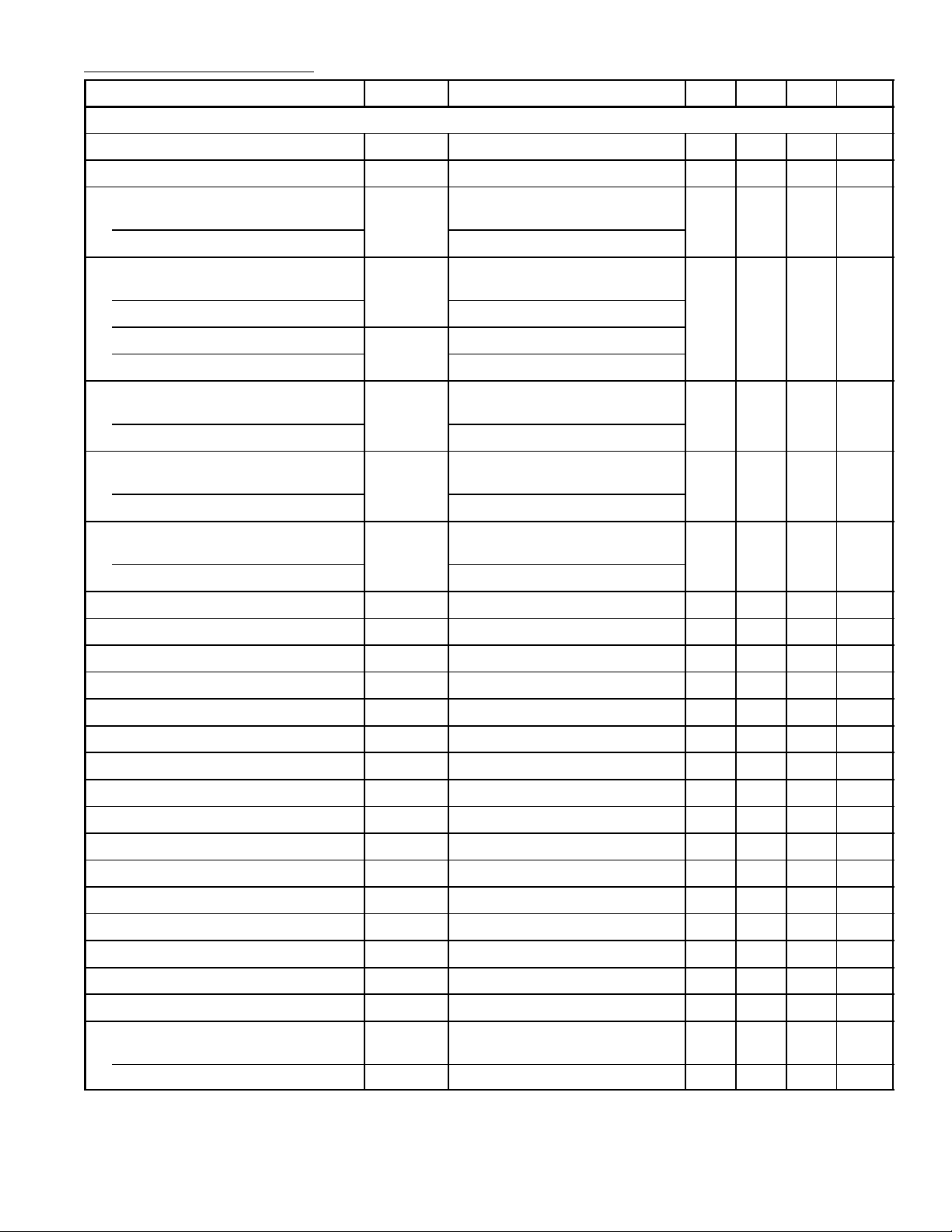
Electrical Characteristics: (TA = +25°C, VCC = 12V, fp = 58.75MHz, fS = 54.25MHz)
Parameter Symbol Test Conditions Min Typ Max Unit
PIF Section
Recommended Supply Voltage V
Supply Current I
CC
CC
Video DC Output Voltage
NTE1570
V
15
SW1: 2, SW2: 2 5.2 5.5 5.8 V
NTE1572 SW1: 1, SW2: 2
AFT DC Output Voltage
NTE1570 V
13
SW1: 2, SW2: 2 5.3 6.8 8.3 V
NTE1572 SW1: 1, SW2: 2
NTE1570 V
14
SW1: 2, SW2: 2
NTE1572 SW1: 1, SW2: 2
AFT DC Offset Voltage
NTE1570 ∆V
13–14
SW1: 2, SW2: 2 –1.5 0 +1.5 V
NTE1572 SW1: 1, SW2: 2
RF AGC Residual Output Voltage
NTE1570 V
11(sat)
SW1: 2, SW2: 2 – – 0.5 V
NTE1572 SW1: 1, SW2: 2
RF AGC Leakage Current
NTE1570 I
11(leak)
SW1: 2, SW2: 1 – – 1.0 µA
NTE1572 SW1: 1, SW2: 1
10.8 12.0 13.2 V
50 72 95 mA
Video Sensitivity (Pin7–Pin8) v
AGC Range ∆A
Sync Tip Level Voltage (V15) V
Maximum IF Input Voltage (PIF) i
SYNC
IN(MAX)
White Noise Threshold Level (V15) V
White Noise Clamp Level (V15) V
Black Noise Threshold Voltage (V15) V
Black Noise Clamp Level (V15) V
Video Frequency Response f
PIF
WTH
WCL
BTH
BCL
BW
Note 1 60 150 250 µV
i
Note 2 60 64 – dB
Note 3 2.3 2.5 2.7 V
Note 4 100 120 – mV
Note 5 5.8 6.2 6.6 V
Note 5 3.7 4.1 4.5 V
Note 5 1.4 1.6 1.8 V
Note 5 2.9 3.3 3.7 V
Note 6 4.5 5.5 – MHz
rms
Suppression of Carrier CL Note 7 40 50 – dB
Suppression of 2nd Carrier I
920kHz Beat Level I
2nd
920
Note 8 40 50 – dB
Note 9 33 38 – dB
Differential Phase DP Note 10 – 3.5 5.0 deg
Differential Gain DG Note 10 – 7 10 %
PIF Input Impedance R
PIF Input Capacitance C
IN(PIF)
IN(PIF)
Note 11 1.5 3.0 6.0 kΩ
Note 11 – 3 10 pF
AFT Output Voltage
Upper V
Lower V
13U
13L
, V
, V
Note 13 11.7 11.9 12.0 V
14U
14L
1.8 2.3 2.8 V
rms

Electrical Characteristics (Cont’d): (TA = +25°C, VCC = 12V, fp = 58.75MHz, fS = 54.25MHz)
Parameter Symbol Test Conditions Min Typ Max Unit
RF AGC Maximum Available Current
NTE1570 I
4(max)
NTE1572 SW1: 1, SW2: 1 0.3 – – mA
SW1: 2, SW2: 1 7.0 – – mA
RF AGC Delay Setting Range (Delay) V
AFT Band Width ∆F
Video Output Voltage v
OUT
SIF Output Voltage S
IN
OUT
Note 14 5 7 9 V
Note 13 1.4 – – MHz
W
Note 15 2.25 2.50 2.75 V
Note 16 200 400 600 mV
SIF Section
Input Limiting Voltage v
IN(LIM)
AM Rejection Ratio AMR SIF IN: f = 4.5MHz, fm = 400Hz,
RD = ∞, Note 17 – 200 400 µV
40 45 – dB
∆f = ±25kHz, AM: 30%,
vin = 100dBµ
Recovered Output Voltage V
OD
SIF IN: f = 4.5MHz, fm = 400Hz,
0.5 0.75 – V
∆f = ±25kHz, vin = 80dBµ,
RD = 12kΩ
Total Harmonic Distortion THD SIF IN: f = 4.5MHz, fm = 400Hz,
– 1.0 – %
∆f = ±25kHz, vin = 80dBµ
Max. Audio Output Voltage v
SIF Input Impedance R
SIF Input Capacitance C
DET Output Impedance R
OM
IN(SIF)
IN(SIF)
O(DET)
SIF IN: f = 4.4 to 4.6MHz 4.0 – – V
f = 4.5MHz 10 20 30 kΩ
f = 4.5MHz – 3.0 – pF
Note 18 10 15 20 kΩ
DC Voltage, Pin21
NTE1570 V
21
SW1: 2, SW2: 2 3.5 4.4 5.3 V
NTE1572 SW1: 1, SW2: 2 3.5 4.4 5.3 V
rms
rms
rms
P–P
DC Voltage, Pin23
NTE1570 V
23
SW1: 2, SW2: 2 4.8 6.0 7.2 V
NTE1572 SW1: 1, SW2: 2 4.8 6.0 7.2 V
DC Voltage, Pin1
NTE1570 V
SW1: 2, SW2: 2 6.0 6.7 7.4 V
1
NTE1572 SW1: 1, SW2: 2 6.0 6.7 7.4 V
Max. Attenuation ATT MAX Note 19 60 – – dB
DC Volume Gain G
ATT Characteristics V
MAX RA = 0 4 6 8 dB
ATT
Note 22 3.4 3.8 4.2 V
1
Note 23 4.5 4.9 5.3 V
Signal Leakage v
PT
Note 20 – 1.0 3.0 mV
AF Amp Gain GV AF Note 21 – 20 – dB
AF Amp Distortion THD AF P
= 1VPP, 400Hz, SW3: ON,
23A
– 1.5 – %
ATT: –26dB Setting
AF Amp Max. Output Voltage v
MAX THDAF = 5%, Note 21 1.5 2.0 – V
OAF
rms
AF Output DC Voltage
NTE1570 V
SW1: 2, SW2: 2 6.7 7.7 8.8 V
3
NTE1572 SW1: 1, SW2: 2 6.7 7.7 8.8 V
rms

Notes:
Note 1. V
Note 2. V
Note 3. PIF IN: f = 58.75MHz CW 15mV
Note 4. PIF IN: f = 58.75MHz, APL 100%, 87.5% AM modulation. P
(P5 EXT. Applying V oltage) = 11.5V, PIF IN: f = 58.75MHz 1kHz 30% AM Modulation.
AGC
Adjust PIF input level (v
be 0.8V
= 4V. Measure PIF input level (vi) same as Note 1.
AGC
and measure the input level.
P–P
(1) Adjust PIF input level 50mV
) so that the detected output of P
i
. Measure DC level of P15.
rms
and measure the detected output level v
P–P
with high impedance probe will
15A
: Ppen.
5
(2) Then increase the input level so that the detected output level will be 1.1 x v
01P–P
01P–P
and measure the input level.
Note 5. V
= 8V. PIF IN: 58.75MHz ±10MHz variable or sweep 15mV
AGC
measure DC level of
rms
P15.
Note 6. V
= 8V (GR = 30dB). SG1: 58.75MHz CW, SG2: 58.65 to 40MHz variable.
AGC
(1) Setting output of SG1 so that DC level of P15 will be 4V.
(2) Setting output of SG2 (58.65MHz) so that AC level of P15 will be 0.5V
(3) Decreaseing frequency of SG2 until AC level of P15 will be 0.35V
(–3dB of 0.5V
) then read f
P–P
= F, fBW = 58.75–F MHz
SG2
Note 7. SG1: 58.75MHz, 1kHz 80% AM modulation 100mV
that output AC level of P15 will be 2.7V
Note 8. Measure I
Note 9. V
= 8V. SG1: 58.75MHz (P = Picture) 100mV
AGC
32mV
rms
(1) Seting V
of P15 same as Note 7.
2nd
(–10dB of SG1). SG3: 55.17MHz (C = Chroma) 32mV
so that the output tip level (lower) of P15 will be 3V DC.
AGC
. Measure CL of P15 after setting to 0% AM of SG1.
P–P
P–P
. SG2, SG3: OFF. Setting V
rms
. SG2: 54.25MHz (S = Sound)
rms
(–10dB of SG1).
rms
P–P
.
AGC
(2) Measure the level difference (dB) between c–level and 920kHz level.
Note10. V
= 8V. PIF IN: f = 58.75MHz video signal (ramp) 87,5% AM 100mV
AGC
. Setting ATT
P–P
so that the sync tip level of P15 will be 2.5V DC. Measure DP and DG.
Note11. V
= 5V, f = 58.75MHz. Measure RIN, CIN.
AGC
Note12. AFT sensitivity ∆F/∆(V13–V14)
(1) INT, AGC (P5 Open)
(2) PIF Input: 58.75MHz ±1MHz, CW 15mV
rms
.
(3) Read the frequency (f1) of PIF when V13–V14 = –1V.
(4) Read the frequency (f2) of PIF when V13–V14 = 1V.
Then calculate ∆F/∆(V13–V14) = |f1–f2|
Note13. ∆FW, V
13U
, V
14U
, V
13L
, V
14L
(1) INT AGC (P5 Open)
(2) PIF IN: 58.75MHz ±10MHz CW 15mV
rms
(3) 9pF at Pin16 should b shorted
(4) Read the frequency (f1 or f2) when the V5 or V6 reduced to 90% level of A or B with
varing the frequency. Then band width is the difference from center requency (f0).
Note14. P5: Open. PIF IN: 58.75MHz CW 20mV
rms
.
(1) Adjust the voltage of Pin3 so that the voltage of Pin4 will be 6V DC.
(2) Measure the volatge at Pin3.
Note15. P5: Open. PIF IN: 58.75MHz, 100% APL 87.5% AM modulation signal amplitude 50mV
Measure detected output voltge (White peak to sync tip).
Note16. P5: Open. SG1: 58.75MHz CW 100mV
. SG2: 54.25MHz CW 25mV
rms
. Measure SIF
rms
(4.5MHz) output voltage at P15.
Note17. SIF IN: f = 4.5MHz, FM f
(1) Adjust SIF input level 100mV
= 400Hz, ∆f = ±25kHz.
MOD
and measure the detected output level vOS.
P–P
(2) Then decrease the input level so that the detected output level will be 3dB down of
vOS and measure the input level.
.
so
P–P
.

Notes (cont’d):
Note 18. Output Impedance
(1) SIF IN: f = 4.5MHz, FM f
= 400Hz, ∆f = ±25kHz, 80dBµ.
MOD
(2) At P23 read the VO1 at RX = ∞, then read the RX when recovered output become
VO1/2 with varying the RX. The RX is the output impedance.
Note19. ATT MAX.
(1) SIF IN: f = 4.5MHz, FM f
= 400Hz, ∆f = ±25kHz, 80dBµ.
MOD
(2) Read the 400Hz component of VA1 at P2 with RA = 0, then read V
Note20. v
PT
(1) SIF IN: f = 4.5MHz, FM f
= 400Hz, ∆f = ±25kHz, 80dBµ.
MOD
(2) Read the 400Hz component at P3.
Note21. GV AF
(1) Apply 400Hz 0.1V
signal to P2.
rms
(2) Read the output voltage at P3.
Note22. Read the 400Hz component of VA1 at P2 with RA = 0. Set RA so that V
then read DC voltage of Pin1 (V1).
Note23. Read the 400Hz component of VA1 at P2 with RA = 0. Set RA so that V
(–50dB), then read DC voltage of Pin1 (V1).
Pin Connection Diagram
with RA = ∞.
A1’
= 1/2VA1 (–6dB),
A1’
= 3.16 x 10⁻³V
A1’
A1
SIF Detector
24
23
De–Emphasis
22
SIF Detector
21
SIF Input
V
20
CC
19 AFT Tank
Video Tank
18
Video Tank
17
AFT Tank
16
Video Output10
15
14
AFT Output 2
AFT Output 112
13
.520
(13.2)
NFB
Max
1
2
3
4
5
6
7
8PIF Input
9
11
Volume Control
Audio Output
Audio GND
IF AGC Filter/
VCR Switch
PIF Input
PIF Input
PIF Input
RF AGC Delay
RF AGC Output
PIF GND
24 13
112
1.300 (33.02)
.100 (2.54)
1.100 (27.94)
.225
(5.73)
Max
.126
(3.22)
Min
.600
(15.24)
 Loading...