

NTE NTE1561 Datasheet
NTE1561
Integrated Circuit
5 LED VU Level Meter
Description:
The NTE1561 is a monolithic integrated circuit in a 9–Lead SIP type package designed for use as a
5 dot LED level meter driver. With a built–in rectifying amplifier, this device is suitable for AC/DC level
meter applications such as VU meters or signal meters.
Features:
D Built–In High Gain Rectifying Amplifier (Av = 26dB)
D Low Radiation Noise when LED Turns On
D Logarithmic Indicator for Bar Type 5 Dot LED (–10, –5, 0, +3, +6dB)
D Constant Current Output: IO = 15mA Typ
D Wide Operating Supply Voltage Range: 3.5V to 16V
D Minimum Number of External Components Required
Absolute Maximum Ratings: (TA = +25°C unless otherwise specified)
Supply Voltage, VCC 18V. . . . . . . . . . . . . . . . . . . . . . . . . . . . . . . . . . . . . . . . . . . . . . . . . . . . . . . . . . . . . . .
Amp Input Voltage, V
Pin7 Voltage, V
7–5
D Terminal Output Voltage, V
Circuit Current, I
CC
D Terminal Output Current, I
. . . . . . . . . . . . . . . . . . . . . . . . . . . . . . . . . . . . . . . . . . . . . . . . . . . . .
8–5
D
D
Power Dissipation, Pd 1100mW. . . . . . . . . . . . . . . . . . . . . . . . . . . . . . . . . . . . . . . . . . . . . . . . . . . . . . . . . .
Derate Above 25°C 11mW/°C. . . . . . . . . . . . . . . . . . . . . . . . . . . . . . . . . . . . . . . . . . . . . . . . . . . . . .
Operating Temperature Range, T
Storage Temperature Range, T
–25° to +80°C. . . . . . . . . . . . . . . . . . . . . . . . . . . . . . . . . . . . . . . . .
opr
–40° to +125°C. . . . . . . . . . . . . . . . . . . . . . . . . . . . . . . . . . . . . . . . . .
stg
–0.5 to V
12mA. . . . . . . . . . . . . . . . . . . . . . . . . . . . . . . . . . . . . . . . . . . . . . . . . . . . . . . . . . . . . . .
20mA. . . . . . . . . . . . . . . . . . . . . . . . . . . . . . . . . . . . . . . . . . . . . . . . . . . . . .
CC
6V. . . . . . . . . . . . . . . . . . . . . . . . . . . . . . . . . . . . . . . . . . . . . . . . . . . . . . . . . . . . . . . . . . .
18V. . . . . . . . . . . . . . . . . . . . . . . . . . . . . . . . . . . . . . . . . . . . . . . . . . . . . . .
Electrical Characteristics: (TA = +25°C, VCC = 6V, f = 1kHz unless otherwise specified)
Parameter Symbol Test Conditions Min Typ Max Unit
Circuit Current I
D Output Current I
Input Bias Current I
Amp Gain A
Comparator ON Level GD
CC
GD
GD
GD
GD
Vi = 0V – 6.0 8.5 mA
Vi = 0.15V 11.0 15.0 18.5 mA
O
B
Vi = 0.1V 24 26 28 dB
v
1
2
Note 1 – 0 – dB
3
4
5
–1 – 0 µA
–12 –10 –8 dB
–6 –5 –4 dB
2.5 3.0 3.5 dB
5.0 6.0 7.0 dB
Note 1. Definition of 0dB: Input voltage level when GD3 turn ON (50mV).
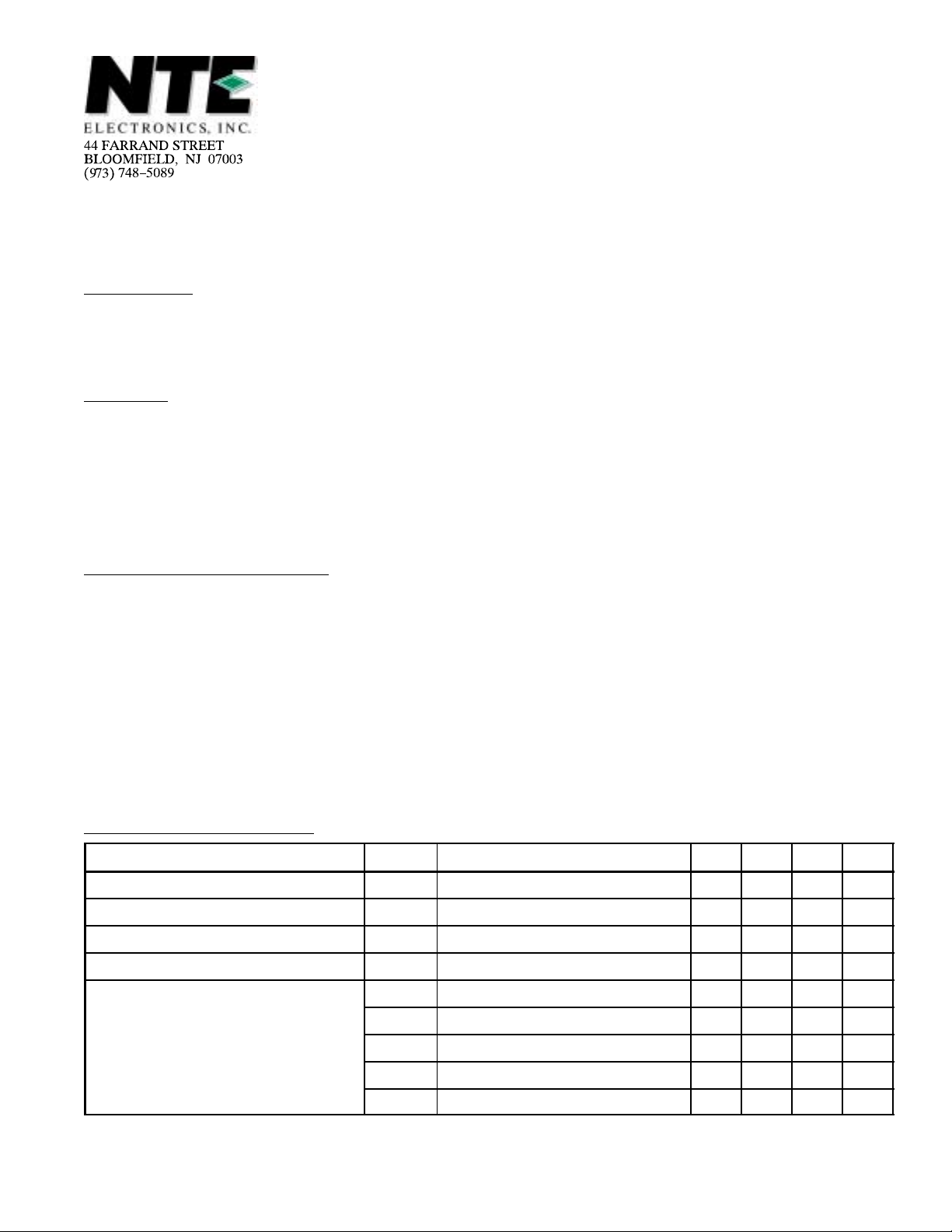
Pin Connection Diagram
(Front View)
9
f
8
7
6
5
4
3 D3
2 D2
1 D1
V
CC
Input
Amp Output
D5
GND
D4
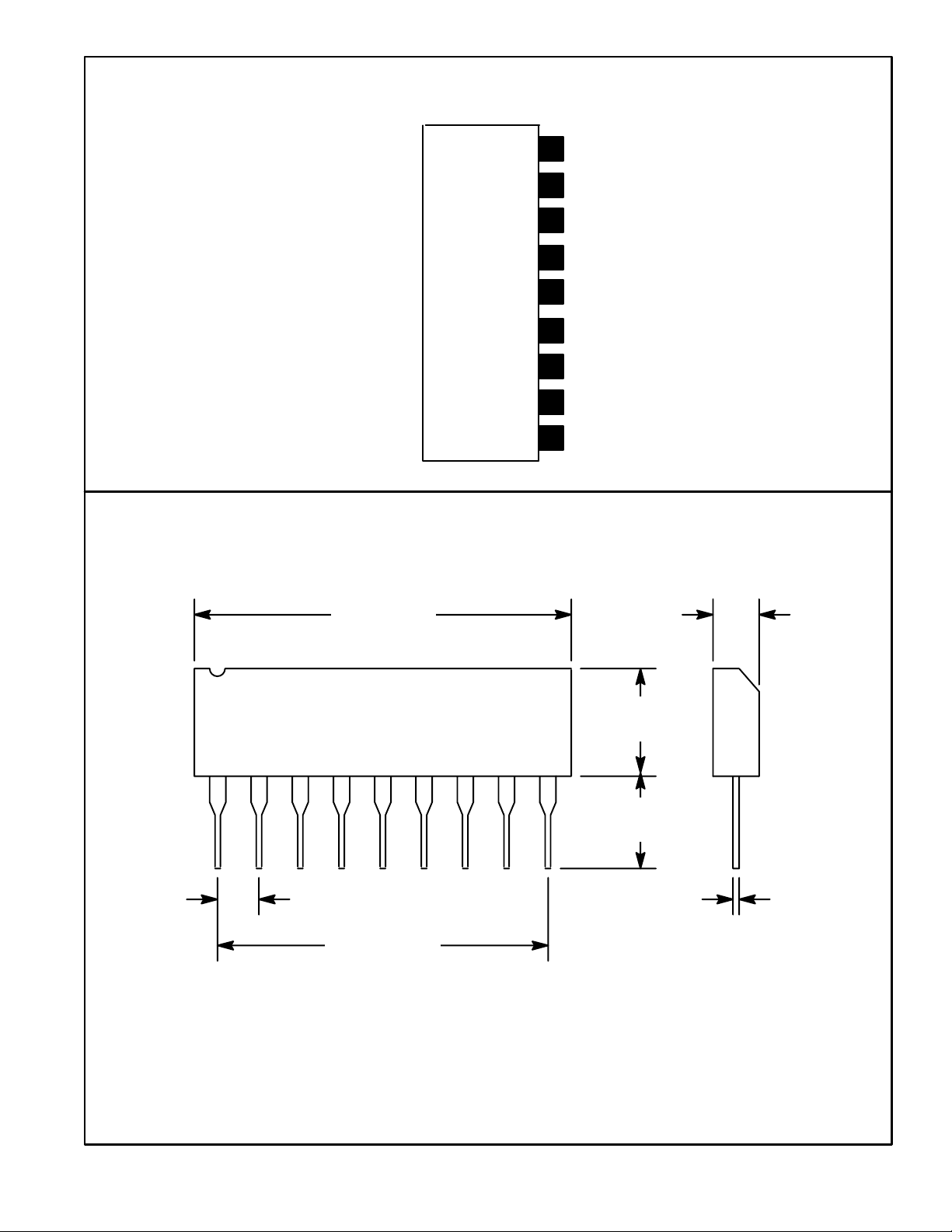
.870 (22.0)
.110 (2.8)
.235
(6.0)
19
.195
(5.0)
.100 (2.54)
.012 (0.30)
.800 (20.32)
 Loading...