

NTE NTE1557 Datasheet

NTE1557
Integrated Circuit
FM/AM IF System
Description:
The NTE1557 is a monolithic integrated circuit in a 16–Lead DIP type package developed for the radio
cassette tape recorder included AM/FM IF amplifier and detector.
Functions:
D AM Section:
IF Amplifier with AGC Detector
D Voltage Regulator for RF External Circuit
D FM Section:
IF Amplifier
Quadrature Detector
Post Amplifier
Signal Meter Driver Circuit
Features:
D Suitable for Radio Cassette and Home Stereo
D Wide Operating Supply Voltage Range (3.0V to 14V)
D Low Quiescent Circuit Current
D AM Section
D Simplified Input Circuit IFT (Ceramic Filter Type)
RF AGC Available
D FM Section:
High Limiting Sensitivity (33dBµ, Typ)
Low Residual Noise (45dB at Vi = –10dBµ)
Small Side Peak of Detuned Output Voltage
Absolute Maximum Ratings: (TA = +25°C unless otherwise specified)
Supply Voltage, V
Power Dissipation, P
Operating Temperature Range, T
Storage Temperature Range, T
CC
D
opr
stg
16V. . . . . . . . . . . . . . . . . . . . . . . . . . . . . . . . . . . . . . . . . . . . . . . . . . . . . . . . . . . . . . . .
600mW. . . . . . . . . . . . . . . . . . . . . . . . . . . . . . . . . . . . . . . . . . . . . . . . . . . . . . . . . . .
–20° to +70°C. . . . . . . . . . . . . . . . . . . . . . . . . . . . . . . . . . . . . . . . .
–40° to +125°C. . . . . . . . . . . . . . . . . . . . . . . . . . . . . . . . . . . . . . . . . .
Electrical Characteristics: (TA = +25°C, VCC = 5.5V, unless otherwise specified)
Parameter Symbol Test Conditions Min Typ Max Unit
FM Section (f = 10.7MHz, fm = 1kHz, ∆f = ±75kHz)
Quiescent Circuit Current I
Input Limiting Sensitivity V
Detector Output Voltage V
Total Harmonic Distortion THD Vi = 100dBµ – 0.3 1.0 %
AM Rejection Ratio AMR Vi = 100dBµ 50 60 – dB
Signal to Noise Ratio S/N Vi = 100dBµ 72 83 – dB
Signal Meter Output V
Residual Noise V
Muting Attenuation M(att) VI = 37dBµ, Mute SW on – 35 – dB
AM Section (f = 455kHz, fm = 1kHz, 30% Mod)
Quiescent Circuit Current I
Maximum Sensitivity Vi(sen) VO (AF) = 10mV – 29 – dBµ
Detector Output Voltage V
Total Harmonic Distortion THD
Signal to Noise Ratio S/N Vi = 74dBµ 45 55 – dBµ
CC
i(lim)
CC
Vi = 0 7 11 16.5 mA
VO (Vi = 100dBµ) –3dB – 33 38 dBµ
VI = 100dBµ 180 245 310 mV
O
Vi = 100dBµ 1.05 1.5 2.05 V
M
VO (AF) (Vi = 100dBµ) – 45 – dB
N
Vi = 0 – 8 – mA
Vi = 74dBµ 45 65 85 mV
o
Vi = 74dBµ – 0.3 2.0 %
Vi = 100dB – 0.7 3.5 %
Signal Meter Output V
Input Impedance (Pin 16) R
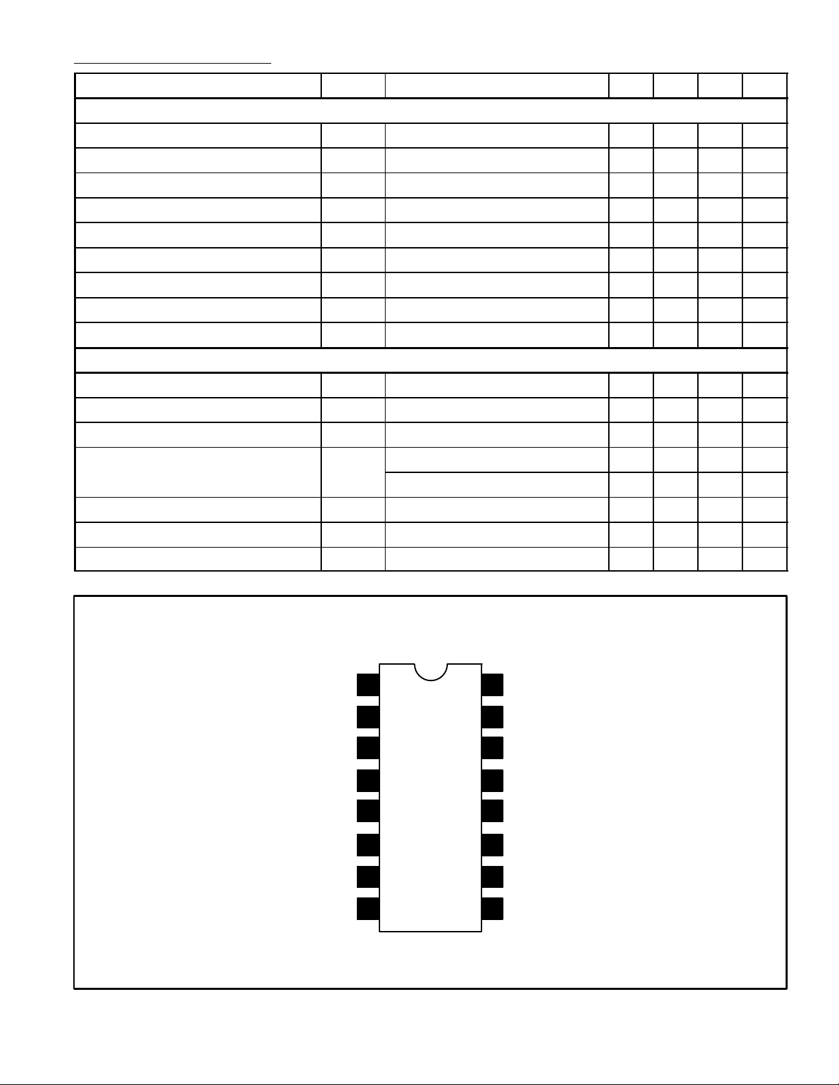
Pin Connection Diagram
1st IF Amp Input (FM)
1st IF Decouple (FM)
VCC (FM)
1st IF Amp Output (FM)
2nd IF Amp Input (FM)
VI = 100dBµ 1.2 1.4 1.6 V
M
Pin 16 0.8–0.9V
i
1
2
3
4
5GND
6
7Voltage Regulator
DC
1st IF Amp Input (AM)
16
15
AGC Decouple
2nd IF Amp Input (AM)
14
13
GND
12 Detector Output
11
V
CC
10 Center Meter
1.45 2.12 2.8 kΩ
8Phase Shifter (FM) 9 FM Output
 Loading...