

NTE NTE1549 Datasheet

NTE1549
Integrated Circuit
Dot/Bar Display Driver
Description:
The NTE1549 is a monolithic integrated circuit that senses analog voltage levels and drives ten LEDs,
LCDs, or vacuum fluorescent displays, providing an electronic version of the popular VU meter. One
pin changes the display from a bar graph to a moving dot display. LED current drive is regulated and
programmable, eliminating the need for current limiting resistors. The whole display system can operate from a single supply as low 3V or as high as 25V.
This IC contains an adjustable voltage reference and an accurate ten–step voltage divider . The high
impedance input buffer accepts signals down to ground and up to within 1.5V of the positive supply.
Further, i t needs no protection against inputs of ±35V. The i n p u t b u ffer drives 10 individual comparators referenced to the precision divider. Accuracy is typically better than 0.2dB.
Audio applications include average or peak level indicators, and power meters. Replacing conventional meters with an LED bar graph results in a faster responding, more rugged display with high visibility that retains the ease of interpretation of an analog display.
The NTE1549 is extremely easy to apply . A 12V full–scale meter requires only one resistor in addition
to the ten LEDs. One more resistor program in addition to the full–scale anywhere from 1.2V to 12V
independent of supply voltage. LED brightness is easily controlled with a single pot.
The NTE1549 is very versatile. The outputs can drive LCDs, vacuum fluorescents and incandescent
bulb as well as LEDs of any color. Multiple devices can be cascaded for a dot or bar mode display
for increased range and/or resolution.
Features:
D Fast responding electronic VU meter
D Drives LEDs, LCDs, or vacuum fluorescents
D Bar or dot display mode externally selectable by user
D Expandable to displays of 70dB
D Internal voltage reference from 1.2V to 12V
D Operates with a single supply of 3V to 25V
D Inputs operate down to ground
D Output current programmable from 1mA to 30mA
D Input withstands ±35V without damabe or false outputs
D Outputs are current regulated, open collectors
D Directly drives TTL or CMOS
D The internal 10–step divider is floating and can be referenced to a wide range of voltages.
Absolute Maximum Ratings:
Power Dissipation (Note 1) 625mW. . . . . . . . . . . . . . . . . . . . . . . . . . . . . . . . . . . . . . . . . . . . . . . . . . . . . . .
Supply Voltage 25V. . . . . . . . . . . . . . . . . . . . . . . . . . . . . . . . . . . . . . . . . . . . . . . . . . . . . . . . . . . . . . . . . . . . .
Voltage on Output Drivers 25V. . . . . . . . . . . . . . . . . . . . . . . . . . . . . . . . . . . . . . . . . . . . . . . . . . . . . . . . . . .
Input Signal Overvoltage (Note 2) ±35V. . . . . . . . . . . . . . . . . . . . . . . . . . . . . . . . . . . . . . . . . . . . . . . . . . .
Divider Voltage –100mV to V
. . . . . . . . . . . . . . . . . . . . . . . . . . . . . . . . . . . . . . . . . . . . . . . . . . . . . . . . . . . .
Reference Load Current 10mA. . . . . . . . . . . . . . . . . . . . . . . . . . . . . . . . . . . . . . . . . . . . . . . . . . . . . . . . . .
Storage Temperature Range –55° to +150°C. . . . . . . . . . . . . . . . . . . . . . . . . . . . . . . . . . . . . . . . . . . . . . .
Lead Temperature (Soldering, 10 seconds) +300°C. . . . . . . . . . . . . . . . . . . . . . . . . . . . . . . . . . . . . . . . .
Note 1. The maximum junction temperature of the NTE1549 is 100°C. Devices must be derated for
operation at elevated temperatures. Junction to ambient thermal resistance is 120°C/W.
Note 2. Pin 5 input current must be limited to ±3mA. The addition of a 39k resistor in series with Pin5
allows ±100V signals without damage.
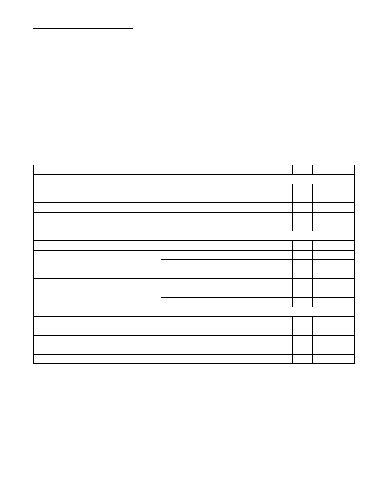
Electrical Characteristics: (Note 3)
Parameter Test Conditions Min Typ Max Unit
Comparators
Offset Voltage, Buffer and First Comparator 0V ≤ V
Offset Voltage, Buffer and Any Other Comparator 0V ≤ V
Gain (∆I
Input Bias Current (At Pin5) 0V ≤ VIN ≤ (V+ =1.5V) – 25 100 nA
Input Signal Overvoltage No Change in Display –35 – +35 V
Voltage Divider
Divider Resistance Total Pin6 to Pin4 8 12 17 kΩ
Relative Accuracy (Input Change Between Any Two
Absolute Accuracy
Voltage Reference
Output Voltage 0.1mA ≤ I
Line Regulation 3V ≤ V+ ≤ 18V – 0.01 0.03 %/V
Load Regulation 0.1mA ≤ I
Output Voltage Change with Temperature 0° ≤ TA ≤ +70°C, I
Adjust Pin Current – 75 120 mA
/∆VIN) I
LED
Threshold Points)
(REF)
–1dB ≤ VIN ≤ 3dB, Note 4 0.75 1.0 1.25 dB
–7dB ≤ VIN ≤ –1dB, Note 4 1.5 2.0 2.5 dB
–10dB ≤ VIN ≤ –7dB, Note 4 2.5 3.0 2.5 dB
VIN = 2, 1, 0, –1dB –0.25 – +0.25 dB
VIN = –3, –5dB –0.5 – +0.5 dB
VIN = –7, –10, –20dB –1 – +1 dB
= V
RLO
= V
RLO
= 2mA, I
L(REF)
L(REF)
≤ 12V, I
RHI
≤ 12V, I
RHI
= 10mA 3 8 – mA/mV
LED
≤ 4mA, V+ = V
≤ 4mA, V+ = V
L(REF)
= 1mA – 3 10 mV
LED
= 1mA – 3 15 mV
LED
= 5V 1.2 1.28 1.34 V
LED
= 5V – 0.4 2.0 %
LED
= 1mA, V+ = V
= 5V – 1 – %
LED
+
Note 3. Unless otherwise stated, all specifications apply with the following conditions:
3VDC ≤ V+ ≤ 20VDC; –0.015V ≤ V
≤ 12VDC; TA = +25°C, IL(REF) = 0.2mA, Pin9 con-
RLO
nected to Pin3 bar mode.
3VDC ≤ V
≤ V+; V
LED
REF
, V
RHI
, V
≤ (V+ –1.5V); For higher power dissipations, pulse
RLO
testing is used.
–0.015V ≤ V
≤ 12VDC; 0V ≤ VIN ≤ V+ –1.5V
RHI
Note 4. Accuracy is measured referred to +3dB = +3dB = +10.000VDC at Pin5, with +10.000VDC at
Pin6, and 0 . 0 0 0 VDC at Pin4. At lower full–scale voltages, buffer and comparator offset voltage may add significant error.
 Loading...