

NTE NTE154 Datasheet

NTE154
Silicon NPN Transistor
High Voltage Video Output
Description:
The NTE154 is a silicon NPN transistor in a TO39 type package designed for use as a video output
to drive a color CRT.
Features:
D High Voltage: V
D Low Capacitance: C
D High Frequency: f
D High Power Dissipation: P
= 300V Min @ IC = 5mA
CEO
= 3pF Max @ VCB = 20V
ob
= 50MHz Min @ IC = 15mA
t
= 7W @ TC = +25°C
D
CBO
EBO
(Note 1)
CEO
300V. . . . . . . . . . . . . . . . . . . . . . . . . . . . . . . . . . . . . . . . . . . . . . . . . . . . .
300V. . . . . . . . . . . . . . . . . . . . . . . . . . . . . . . . . . . . . . . . . . .
7V. . . . . . . . . . . . . . . . . . . . . . . . . . . . . . . . . . . . . . . . . . . . . . . . . . . . . . . .
D
Absolute Maximum Ratings:
Collector to Base Voltage, V
Collector to Emitter Voltage (Note 2), V
Emitter to Base Voltage, V
Total Power Dissipation (Note 3, Note 4), P
TC = +25°C 7W. . . . . . . . . . . . . . . . . . . . . . . . . . . . . . . . . . . . . . . . . . . . . . . . . . . . . . . . . . . . . . . . . .
T
= +25°C 1W. . . . . . . . . . . . . . . . . . . . . . . . . . . . . . . . . . . . . . . . . . . . . . . . . . . . . . . . . . . . . . . . . .
A
Operating Junction Temperature, T
Storage Temperature Range, T
opr
stg
Lead Temperature (During Soldering, 60sec), T
–65° to +200°C. . . . . . . . . . . . . . . . . . . . . . . . . . . . . . . . . . . . . . . . . .
L
+200°C. . . . . . . . . . . . . . . . . . . . . . . . . . . . . . . . . . . . . . . . . . . . . .
+300°C. . . . . . . . . . . . . . . . . . . . . . . . . . . . . . . . . . . .
Note 1. These rati ng s a r e l i mit in g v al ue s a b ove whic h t h e s e rvi ceability o f t his d evice m ay b e i mpaired.
Note 2. This rating refers to a high current point where collector to emitter voltage is lowest.
Note 3. These ratings are steady state limits.
Note 4. These ratings give a maximum junction temperature of +200°C and junction to case thermal
resistance of + 2 5°C/W (derating factor of 40mW/°C); junction to ambient thermal resistance
of +175°C/W (derating factor of 5.71mW/°C).
Electrical Characteristics: (TA = +25°C unless otherwise specified)
Parameter Symbol Test Conditions Min Typ Max Unit
Collector Base Breakdown Voltage V
Emitter Base Breakdown Voltage V
(BR)CBOIC
(BR)EBOIE
Collector Cutoff Current I
Emitter Cutoff Current I
DC Current Gain h
Collector Emitter Sustaining Voltage V
Base Emitter Saturating Voltage V
Collector Emitter Saturating Voltage V
CEO(sus)IC
BE(sat)IC
CE(sat)IC
High Frequency Current Gain h
Collector Base Capacitance C
Emitter Base Capacitance C
CBO
EBO
FE
fe
cb
eb
= 100µA, IE = 0 300 – – V
= 100µA, IC = 0 7 – – V
IE = 0, VCB = 200V – 1.0 100 nA
IE = 0, VCB = 200V, TA = +125°C – 0.2 5.0 µA
IC = 0, VEB = 6V – 1.0 100 nA
IC = 1mA, VCE = 20V 20 50 –
IC = 10mA, VCE = 20V, Note 5 40 100 –
IC = 30mA, VCE = 20V, Note 5 40 100 –
= 5mA, IB = 0, Note 2, Note 5 300 – – V
= 20mA, IB = 2mA, Note 5 – 0.74 0.85 V
= 20mA, IB = 2mA, Note 5 – 0.35 1.0 V
IC = 15mA, VCE = 150V, f = 20MHz 2.5 4.0 –
IC = 3mA, VCE = 270V, f = 20MHz 2.0 2.5 –
IC = 30mA, VCE = 30V, f = 20MHz,
= 9kΩ
R
L
2.0 4.0 –
IE = 0, VCB = 20V – 2.5 3.0 pF
IC = 0, VEB = 500mV – 45 70 pF
Note 2. This rating refers to a high current point where collector to emitter voltage is lowest.
Note 5. Pulse Conditions: Length = 300µs, Duty Cycle = 1%.
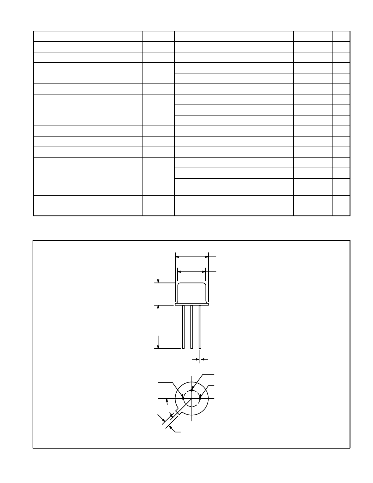
.370 (9.39) Dia Max
.355 (9.03) Dia Max
.260
(6.6)
Max
.500
(12.7)
Min
.018 (0.45)
Base
Emitter
Collector/Case
45°
.031 (.793)
 Loading...