

NTE NTE1536 Datasheet

NTE1536
Integrated Circuit
CB Transceiver PLL Frequency Synthesizer
Description:
The NTE1536 is a CMOS LSI device for the 27MHZ Citizen’s Band Transceiver.
Function:
The NTE1536 composes a Phase Lock Loop (PLL) frequency synthesizer system with only one
crystal for an AM CB transceiver.
Features:
D Only one crystal is required for AM CB transceiver.
D Two types of intermediate frequency can be selected:
IF1 = 10.695MH
IF2 = 9.785MH
D Two types of lock monitor outputs:
LM: When PLL is locked/unlocked, LM is high/low level.
LM: When PLL is locked/unlocked, LM is low/high level.
D The amplifier for low pass filter.
D The amplifier for programmable counter input.
D The detecting circuit for the mis–programming.
D BCD code input to the programmable counter.
D The buffer output for the reference oscillator.
D The output for the half frequency of the reference oscillator.
D The reference frequency oscillation amplifier (with feedback resistance).
Z
Z
Absolute Maximum Ratings: (TA = +25°C unless otherwise specified)
Maximum Supply Voltage, VDDmax –0.3 to +9.0V. . . . . . . . . . . . . . . . . . . . . . . . . . . . . . . . . . . . . . . . . .
Input Voltage, V
Output Voltage, V
IN
(Unload) –0.3 to VDD+0.3V. . . . . . . . . . . . . . . . . . . . . . . . . . . . . . . . . . . . . . . . . . .
OUT
Operating Temperature Range, T
Storage Temperature Range, T
stg
opg
–0.3 to VDD+0.3V. . . . . . . . . . . . . . . . . . . . . . . . . . . . . . . . . . . . . . . . . . . . . . . . . . . . . .
–30° to +70°C. . . . . . . . . . . . . . . . . . . . . . . . . . . . . . . . . . . . . . . . .
–40° to +125°C. . . . . . . . . . . . . . . . . . . . . . . . . . . . . . . . . . . . . . . . . .
Available Operation Conditions: (TA = +25°C, VDD = 7V ±1V unless otherwise specified)
Parameter Symbol Test Conditions Min Typ Max Units
Supply Voltage V
High Level Input Voltage V
Low Level Input Voltage V
DD
IH
IL
Input Amplitude VIN (1) 10.25MHZ, Duty 50±10% Sine Wave 3.0 – 0.9V
VIN (2) 3.5MHZ, Duty 50±10% Sine Wave 0.7 – 0.66V
Input Frequency f
(1) 3.0Vp–p, Duty 50±10% Sine Wave – – 10.25 MH
IN
6.0 7.0 8.0 V
VDD–1.5 – – V
– – 1.5 V
Vp–p
DD
Vp–p
DD
fIN (2) 0.7Vp–p, Duty 50±10% Sine Wave – – 3.5 MH
Electrical Characteristics: (TA = +25°C, VDD = 7V ±1V unless otherwise specified)
Parameter Symbol Test Conditions Min Typ Max Units
Feedback Resistance Rf (1) – 7.0 – MΩ
Rf (2) – 3.0 – MΩ
Pull–Down Resistance RP – 28 – kΩ
Input Floating Voltage V
3 State Off Leak Current I
Output Off Leak Current I
OFF
OFF
I
OFF
Input Current I
Filter Amp Gain VG Rf = 1MΩ, fIN = 10kHZ, Rg = 600Ω – 28 – dB
Pin Opened – 1.0 – V
IF
(1) VO = VDD/2 – 1.0 – nA
(2) VO = V
(3) VO = V
VI = VDD, VI = V
IN
DD
SS
SS
– – 3.0 µA
– – 3.0 µA
– 1.0 – nA
Z
Z
Low Level Output Voltage V
High Level Output Voltage V
Dissipation Current I
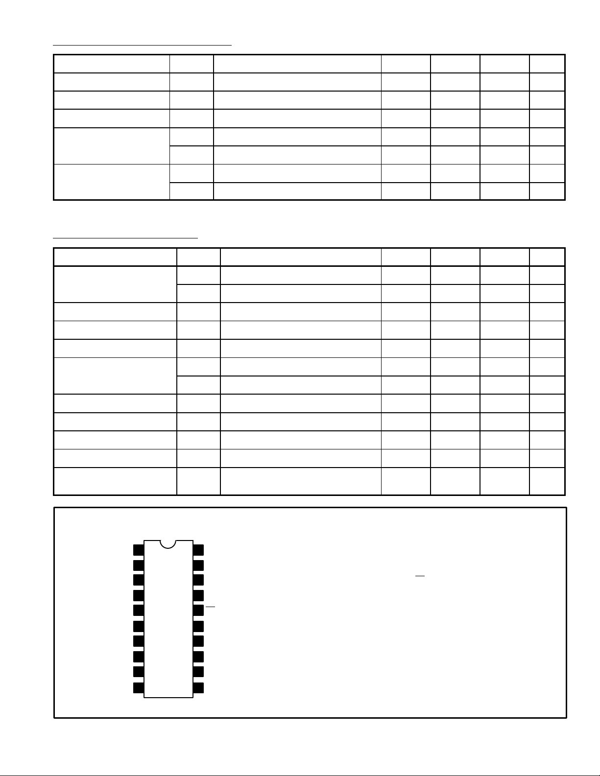
Pin Connection Diagram
1
D1
2
D2
3
D3
4
D4
D5
5
D6
6
7
IFS
8
T/R
9
V
DD
10
X IN
IO = 2mA – – 0.9 V
OL
OHIO
DD
fIN (1) = 10.24MHZ,
fIN (2) = 3.5MHZ, N = 182
V
20
SS
A
19
OUT
A
18
IN
17 PD OUT
16
LM
15
LM
14
PC IN
1/2 R OUT
13
R OUT
12
11
X OUT
= 5mA VDD–0.9 – – V
– – 20 mA
Pin Functions
D1 – D6 Program Input (BCD) 1/2 R OUT 1/2 Freq of Ref Osc
IFS 10.695/9.785MH
T/R TX/RX Sw LM
V
DD
X IN Crystal Oscillator A
X OUT Crystal Oscillator A
R OUT Buffer Output of Ref Osc V
D1: LSB, D6: MSB PC IN Programmable Divider Input
Supply Voltage PD OUT Phase Detector Output
Sw LM Lock Monitor Output
Z
IN
OUT
SS
Lock Monitor Output
Filter Amp Input
Filter Amp Output
GND
 Loading...