

NTE NTE1534 Datasheet
NTE1534
Integrated Circuit
CMOS, Phase Lock Loop (PLL) Frequency
Synthesizer for AM/FM Radio
Description:
The NTE1534 is a CMOS PLL frequency synthesizer in a 16–Lead DIP type package designed for
FM–AM radios. This device contains a reference counter, programmable counter, and phase
comparator circuits.
Absolute Maximum Ratings: (VSS = 0, TA = +25°C unless otherwise specified)
Supply Voltage, V
Input Voltage, V
Output Voltage, V
Power Dissipation, P
Operating Temperature Range, T
Storage Temperature Range, T
DD
I
O
D
opr
stg
Operating Conditions: (VSS = 0, TA = –20° to +70°C unless otherwise specified)
–0.3 to +10V. . . . . . . . . . . . . . . . . . . . . . . . . . . . . . . . . . . . . . . . . . . . . . . . . . . . . . . .
–0.3 to VDD+0.3V. . . . . . . . . . . . . . . . . . . . . . . . . . . . . . . . . . . . . . . . . . . . . . . . . . . . . . .
–0.3 to VDD+0.3V. . . . . . . . . . . . . . . . . . . . . . . . . . . . . . . . . . . . . . . . . . . . . . . . . . . . .
50mW. . . . . . . . . . . . . . . . . . . . . . . . . . . . . . . . . . . . . . . . . . . . . . . . . . . . . . . . . . . .
–20° to +70°C. . . . . . . . . . . . . . . . . . . . . . . . . . . . . . . . . . . . . . . . .
–55° to +100°C. . . . . . . . . . . . . . . . . . . . . . . . . . . . . . . . . . . . . . . . . .
Parameter Symbol Test Conditions Min Typ Max Unit
Supply Voltage V
DD
5.5 6.0 6.5 V
Electrical Characteristics: (TA = –20° to +70°C unless otherwise specified)
Parameter Symbol Test Conditions Min Typ Max Unit
Supply Current I
Total Power Dissipation P
P0 to P3, C0 to C2, LD
Input Voltage Level, “H” V
Input Voltage Level, “L” V
Input Current I
PI
Input Voltage V
Input Current I
Input Frequency f
DD
I(1)
I(2)
VDD = 5V, TA = +25°C – 3 5 mA
VDD = 5V, TA = +25°C – 15 25 mW
tot
VDD = 5V 2.4 – V
IH
IL
VI = VSS to V
I
VI = 0 ±1 ±5 ±25 V
VDD = 5.5V to 6.5V 6 – – MHz
i
DD
V
1.0 – – V
DD
SS
– – ±10 µA
– 0.8 V
V
P–P
P–P
Electrical Characteristics (Cont’d): (TA = –20° to +70°C unless otherwise specified)
Parameter Symbol Test Conditions Min Typ Max Unit
OSC 1, OSC 2
Oscillator Frequency f
OSC
PD
Output Current Level, “H” I
Output Current Level, “L” I
Output Current (Open) I
CPO, QO
Output Voltage Level, “H” V
Output Voltage Level, “L” V
Capacitance
Input Capacitance C
Output Capacitance C
PI Input
OH
OL
OH
OL
VDD = 5V, VO = 3V –0.8 – – mA
VDD = 5V, VO = 2V 0.8 – – mA
VDD = 5V, VO = VSS to V
O
VDD = 5V, IOH = –100µA 4.0 – – V
VDD = 5V, IOL = 100µA – – 0.4 V
VI = 2V – 5 – pF
I
VO = 2V – 7 – pF
O
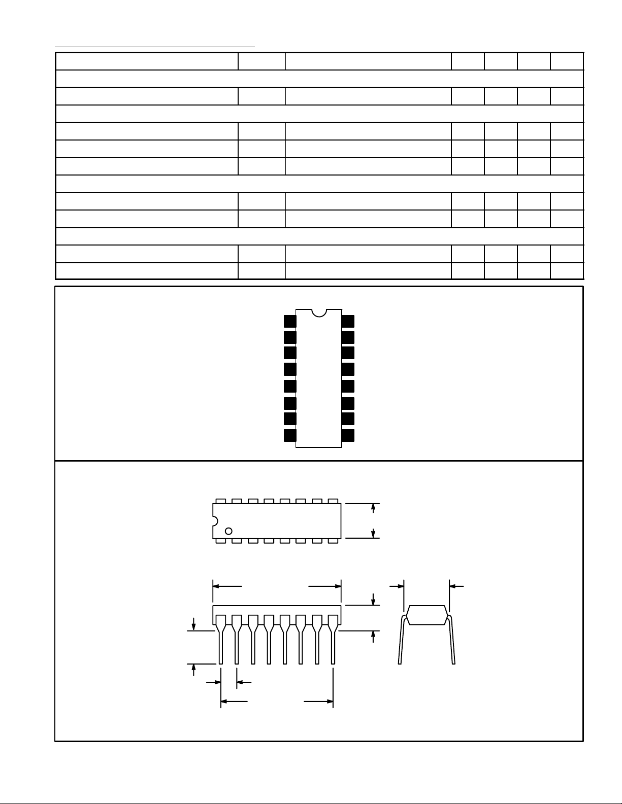
Pin Connection Diagram
V
DD
P312
P2
P1
3
4
5
16
15
14
13
12
V
SS
LD
P0
C0 Input
C1 Input
DD
– 11.52 – MHz
– – ±10 µA
.245
(6.22)
Min
OSC 1 Input
OSC 2 Input
QO Output
16 9
18
6
7
8
.785 (19.9)
Max
.100 (2.54)
C2 Input
11
PD Output
10
CPO Output
9
.260 (6.6) Max
.200 (5.08)
Max
.300
(7.62)
.700 (17.7)
 Loading...