

NTE NTE1531 Datasheet

NTE1531
Integrated Circuit
Voltage Regulator for Electronic Tuning System
Description:
The NTE1531 is a voltage regulator for use with a varactor tuner or electronic tuning control.
Absolute Maximum Ratings: (TA = +25°C unless otherwise specified)
Maximum Input Voltage (+B1, +B2, CLK), VB1, VB2, V
max 21V. . . . . . . . . . . . . . . . . . . . . . . . . . . .
CLK
Allowable Power Dissipation, PDmax 1W. . . . . . . . . . . . . . . . . . . . . . . . . . . . . . . . . . . . . . . . . . . . . . . . .
Operating Temperature Range, T
Storage Temperature Range, T
stg
opg
–20° to +70°C. . . . . . . . . . . . . . . . . . . . . . . . . . . . . . . . . . . . . . . . .
–40° to +125°C. . . . . . . . . . . . . . . . . . . . . . . . . . . . . . . . . . . . . . . . . .
Recommended Operation Conditions: (TA = +25°C unless otherwise specified)
Parameter Symbol Min Typ Max Unit
V
Output Current I
ref
VDD Output Current I
INHI Output Current I
BUC Output Current I
ref
DD
INHI
BUC
+B1, +B2 Input Voltage VB1, V
–10 – 0 mA
–30 – 0 mA
–0.5 – 0 mA
–0.8 – 0 mA
B2
9 – 16 V
Operational Characteristics: (TA = +25°C, unless otherwise specified)
Parameter Symbol Conditions Min Typ Max Unit
VDD Voltage V
DD(1)
+B1 = +B2 = 9V, IDD = 30mA,
I
= 10mA, V
ref
T
= –20° to +70°C
A
= 8V,
ref
V
–0.3 – 8.5 V
ref
VDD Voltage
(At Back–Up Time)
VDD Voltage V
V
DD(2)
V
DD(3)
DD(4)
+B1 = +B2 = 16V, IDD = 30mA,
I
= 10mA, V
ref
T
= –20° to +70°C
A
= 8V,
ref
+B2 = 9 to 16V, IDD = 4mA,
+B
opened.
1
V
= +B2 = 9V, IDD = 18mA,
CLK
I
= 10mA, V
ref
T
= –20° to +70°C, +B1 opened.
A
= 8V,
ref
V
–0.3 – 10 V
ref
4.5 – 5.5 V
V
–0.3 – 8.5 V
ref
Operational Characteristics (Cont’d): (TA = +25°C, unless otherwise specified)
Parameter Symbol Conditions Min Typ Max Unit
VDD Voltage V
Radio Back–Up
Signal Voltage
Clock Back–Up
Signal Voltage
Radio Back–Up Signal
V
Rise Voltage
Radio Back–Up Signal
V
Hysteresis
BUC Delay Time
at +B Step Input
Current Dissipation I
V
Thermal Drift |∆V
ref
Logic Table:
DD(5)
V
BUC
V
INHI
TH BUC
TH BUC
t
D
CC(1)
I
CC(2)
ref
V
= +B2 = 16V, IDD = 18mA, I
CLK
= 10mA, V
T
= –20° to +70°C, +B1 opened.
A
= 8V,
ref
+B1 = +B2 = 9.15 to 16V, V
+B1 = +B2 = 9.15 to 16V, V
+B1 = +B2, V
UP
+B1 = +B2, V
DN
= 8V, I
ref
= 8V, I
ref
+B1 = +B2 = 13.2V,
= 8V 0.78V
ref
= 8V 0.78V
ref
= 10mA 8.9 – 9.3 V
ref
= 10mA 50 – 200 mV
ref
ref
V
–0.3 – 10 V
ref
DD
DD
– V
– V
85 – 400 ms
C = 22µF, R = 22k ohm
+B1 = +B2 = 13.2V,
I
= 30mA, I
DD
= 10mA
ref
– 70
+B2 = 13.2V, no load, +B1 opened. – 0.63 1.4 mA
| TA = –10 to +60°C,
V
= 8V (25°C)
ref
–60 0 60 mV
DD
DD
–
V
V
mA
B1 B2 CLK V
DD
V
ref
BUC INHI Condition
L H L 5V 0V L L When back–up of time
H H L 9V 8V H H radio on
L H H 9V 8V L H read out time when radio off
H H H 9V 8V H H read out time when radio on
NOTE: This device is for REPLACEMENT ONLY! No application notes are available.
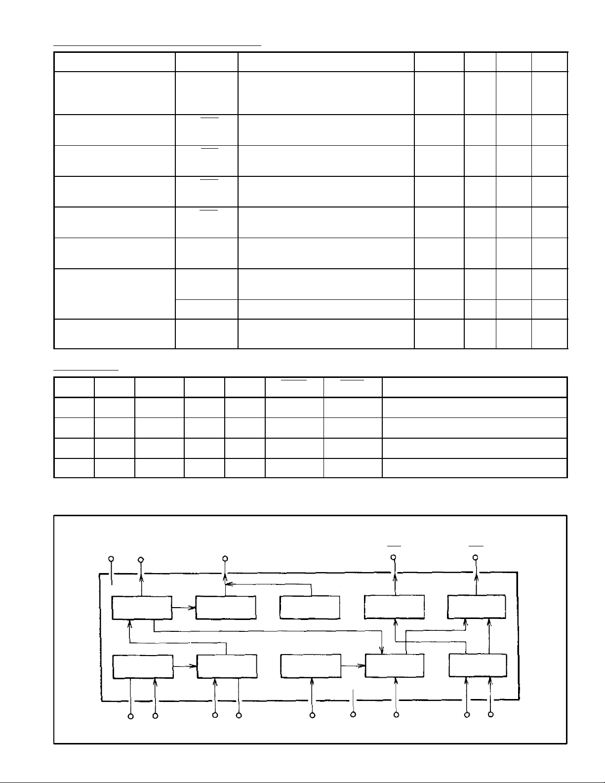
Block Diagram
N.C. V
14 13 12
ref
V
ref
Generator
Reference
Voltage
Generator
V
DD
V
DD
Generator
Comparator
Generator
V
DD
for Back–Up
Time
Delay
INHI BUC
98
Counter IC
Control Signal
Generator
Comparator
Control LSI
Control Signal
Generator
Logic
Circuit
14 23 10
C2 V1 Det C3 C1 GND B
511 67
2
CLK B
1
 Loading...