

NTE NTE1508 Datasheet

NTE1508
Integrated Circuit
10–Step Dot/Bar Display Driver
for Linear Scale
Description:
The NTE1508 is a monolithic integrated circuit in an 18–Lead DIP type package that senses analog
voltage levels a nd dr ives 10 LEDs, providing a l inear a nalog di splay. A s ingle pin c hanges the display
from a moving dot to a b ar g raph. C ur rent d rive t o t he L EDs i s r egul ated a nd p rogr ammable, e lim inating
the need f or r esi stors. T his f eatur e is one that a l lows o peration o f the whole system f rom l ess t han 3 V.
The circuit contains its own adjustable reference and accurate 10–step voltage divider. The low–
bias–current input buffer accepts signals down to GND, or V–, yet needs no protection against inputs
of 35V above or below GND. The buffer drives 10 individual comparators referenced to the precision
divider. Indication non–linearity can thus be held typically to 1/2%, even over a wide temperature
range.
V ersatility was d esigned i nto t he N T E1508 s o t hat c ontroller, v isual a larm, a nd e xpanded s cale f unctions
are easily added on to the display system. The circuit can drive LEDs of many color, or low–current
incandescent lamps. M any NTE1508s c an be “chained” to f orm d isplays of 2 0 to over 100 s egments.
Both e nds o f t he v oltage d ivider a re e xternall y available s o t hat 2 d rivers c an b e m ade i nto a z ero–center
meter.
The NTE1508 is very easy to apply as an analog meter circuit. A 1.2V full–scale meter requires only
1 resistor and a single 3V to 15V supply in addition to the 10 display LEDs. If the 1 resistor is a pot,
it becomes the LED brightness control
When in the dot mode, there is a small amount of overlap or “fade” (about 1mV) between segments.
This assures that at no time will all LEDs be “OFF”, and thus any ambiguous display is avoided. Various novel displays are possible.
Much of the display flexibility derives from the fact that all outputs are individual, DC regulated currents. Various effects can be achieved by modulating these currents. The individual outputs can drive
a transistor as well as a LED at the same time, so controller functions including “staging” control can
be performed. The NTE1508 can also act as a programmer, or sequencer.
Features:
D Drives LEDs, LCDs or vacuum fluorescents
D Bar or dot display mode externally selectable
by user
D Expandable to displays of 100 steps
D Internal voltage reference from 1.2V to 12V
D Operates with single supply of less than 3V
D Inputs operate down to GND
D Output current programmable from 2 to 30mA
D No multiplex switching or interaction between
outputs
D Input withstands ±35V without damage or false
outputs
D LED driver outputs are current regulated,
open–collectors
D Outputs can interfere with TTL or CMOS logic
D The internal 10–step divider is floating and can
be referenced to a wide range of voltages
Absolute Maximum Ratings:
Power Dissipation (Note 1) 1365mW. . . . . . . . . . . . . . . . . . . . . . . . . . . . . . . . . . . . . . . . . . . . . . . . . . . . .
Supply Voltage 25V. . . . . . . . . . . . . . . . . . . . . . . . . . . . . . . . . . . . . . . . . . . . . . . . . . . . . . . . . . . . . . . . . . . .
Voltage on Output Drivers 25V. . . . . . . . . . . . . . . . . . . . . . . . . . . . . . . . . . . . . . . . . . . . . . . . . . . . . . . . . .
Input Signal Overvoltage (Note 2) ±35V. . . . . . . . . . . . . . . . . . . . . . . . . . . . . . . . . . . . . . . . . . . . . . . . . . .
Divider Voltage –100mV to V+. . . . . . . . . . . . . . . . . . . . . . . . . . . . . . . . . . . . . . . . . . . . . . . . . . . . . . . . . . .
Reference Load Current 10mA. . . . . . . . . . . . . . . . . . . . . . . . . . . . . . . . . . . . . . . . . . . . . . . . . . . . . . . . . .
Storage Temperature Range –55° to +150°C. . . . . . . . . . . . . . . . . . . . . . . . . . . . . . . . . . . . . . . . . . . . . .
Lead Temperature (During soldering, 10sec) +260°C. . . . . . . . . . . . . . . . . . . . . . . . . . . . . . . . . . . . . . .
Note 1. The maximum junction temperature of the NTE1508 is +100°C. Device must be derated for
operation at elevated temperatures. Junction to ambient thermal resistance is 55°C/W.
Note 2. Pin5 input current must be limited to ±3mA. The addition of a 39kΩ resistor in series with
Pin5 allows ±100V signals without damage.
Electrical Characteristics: (Note 2, unless otherwise specified, all specifications apply with the
following conditions:
3VDC ≤ V+ ≤ 20V
3VDC ≤ V
–0.015V ≤ V
–0.015V ≤ V
≤ V+ 0V ≤ VIN ≤ V+ –1.5V
LED
RLO
≤ 12V
RHI
DC
≤ 12V
DC
DC
V
, V
REF
TA +25°C, I
V
= 3V, Pin9 connected to Pin3
LED
RHI
, V
RLO
L(REF)
≤ (V+ –1.5V)
= 0.2mA,
(Bar Mode)
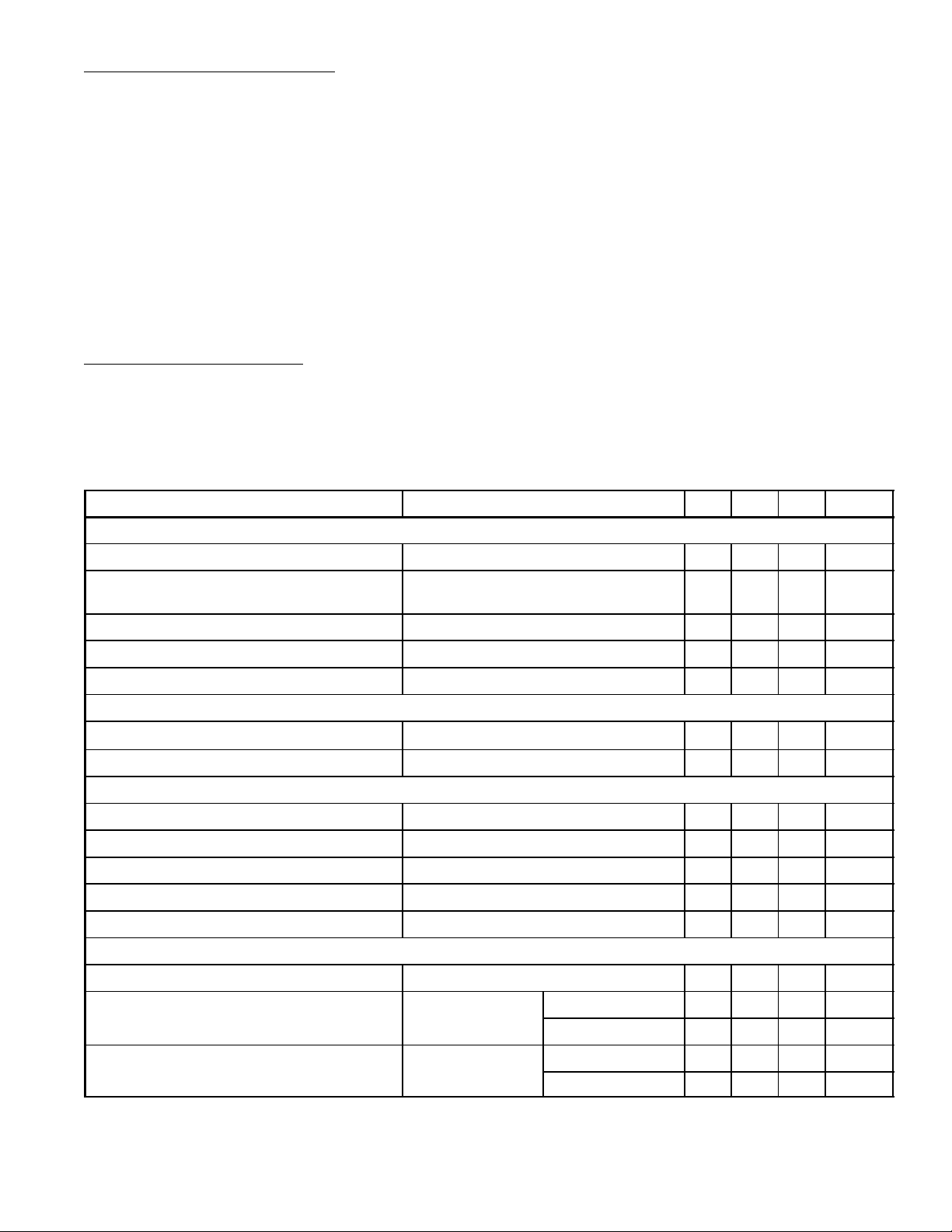
Parameter Test Conditions Min Typ Max Unit
Comparator
Offset Voltage, Buffer, and First Comparator 0V ≤ V
Offset Voltage, Buffer, and Any Other
Comparator
Gain (∆I
Input Bias Current (At Pin5) 0V ≤ VIN ≤ V+ =1.5V – 25 100 nA
Input Signal Overdrive No Change is Display –35 – +35 V
Voltage Divider
Divider Resistance Total, Pin6 to Pin4 8 12 17
Accuracy Note 3 – 0.5 2.0 %
Voltage Reference
Output Voltage 0.1mA ≤ I
Line Regulation 3V ≤ V+ ≤ 18V – 0.01 0.03 %/V
Load Regulation 0.1mA ≤ I
Output Voltage Change with Temperature 0° ≤ TA ≤ +70°C, I
Adjust Pin Current – 75 120 µA
Output Drivers
LED Current V+ = V
LED Current Difference (Between Largest and V
Smallest LED Currents)
LED Current Regulation 2V ≤ V
/∆VIN) I
LED
0V ≤ V
L(REF)
LED
= V
RLO
= V
RLO
= 2mA, I
L(REF)
L(REF)
= 5V, I
LED
= 5V
≤ 17V
LED
≤ 12V, I
RHI
≤ 12V, I
RHI
= 10mA 3 8 – mA/mV
LED
≤ 4m A, V+ = V
≤ 4m A, V+ = V
L(REF)
L(REF)
I
LED
I
LED
I
LED
I
LED
= 1mA – 3 10 mV
LED
= 1mA – 3 15 mV
LED
= 5V 1.2 1.28 1.34 V
LED
= 5V – 0.4 2.0 %
LED
= 1mA, V+ = 5V – 1 – %
= 1mA 7 10 13 mA
= 2mA – 0.12 0.4 mA
= 20mA – 1.2 3.0 mA
= 2mA – 0.1 0.25 mA
= 20mA – 1 3 mA
kΩ
Note 3. Accuracy is measured referred to +10.000VDC at Pin6, with 0.000VDC at Pin4. At lower full–
scale voltages, buffer and comparator offset voltage may add significant error.
 Loading...