


NTE1507
Integrated Circuit
10–Step Adjustable Analog Level Detector
Description:
The NTE1507 is an integrated circuit in a 16–Lead DIP type package consisting of ten comparators
and a reference voltage network to detect the level of a signal at the analog input. Output Q1 is
switched to a low logic level at a typical input voltage of 200mV with Threshold Adjust open and the
cascade input grounded. After each 200mV increment, the next output is switched to a low logic level.
All outputs are at low logic levels at a typical input voltage of 2000mV. The threshold–adjust pin allows
the user to decrease the input voltage steps from 200mV to 100mV increments by connecting an external resistor from Threshold Adjust to GND.
This level detector is directly cascadable requiring only two external resistors to establish a zero–reference level voltage for the cascade input. The maximum number of devices that can be cascaded
is determined by the threshold level and the maximum input voltages. If the cascade feature is not
utilized, the cascade input must be grounded for proper operation.
The NTE1507 is especially designed to detect and indicate analog signal levels and may be used in
various industrial, consumer, or automotive applications such as low–precision meters, warning–signal indicators, A/D converters, feedback regulators, pulse shapers, delay elements, and for automatic
range switching. The open–emitter outputs are capable of sourcing currents up to 25mA and may
be operated at voltages up to 35V . The power outputs are suitable for driving a variety of display elements such as vacuum flourescent displays, LED’s, or filament lamps. The outputs may also drive
digital integrated logic such as CMOS or other high–level logic.
Features:
D 10 Comparators to Digitize Analog Input Signals
D Cascade Feature Allows Stacking Output Display Strings
D Threshold Intervals Adjustable from 200mV to 100mV
D Open–Emitter Outputs Capable of Sourcing up to 25mA and Withstanding up to 35V
D Supply Voltage Range of 10V to 35V (V
CC2
)
Absolute Maximum Ratings: (TA = 0° to +70°C unless otherwise specified)
Supply Voltage
V
(Note 1) 20V. . . . . . . . . . . . . . . . . . . . . . . . . . . . . . . . . . . . . . . . . . . . . . . . . . . . . . . . . . . . . . . .
CC1
V
CC2
Input Voltage
Analog Input 8V. . . . . . . . . . . . . . . . . . . . . . . . . . . . . . . . . . . . . . . . . . . . . . . . . . . . . . . . . . . . . . . . . .
Cascade Input 8V. . . . . . . . . . . . . . . . . . . . . . . . . . . . . . . . . . . . . . . . . . . . . . . . . . . . . . . . . . . . . . . .
Output Voltage Range 0V to V
. . . . . . . . . . . . . . . . . . . . . . . . . . . . . . . . . . . . . . . . . . . . . . . . . . . . . . . .
On–State Output Current (Each Output) –30mA. . . . . . . . . . . . . . . . . . . . . . . . . . . . . . . . . . . . . . . . . . . .
Continuous Total Dissipation (TA ≤ +25°C) 2075mW. . . . . . . . . . . . . . . . . . . . . . . . . . . . . . . . . . . . . . . .
Derate Linearly Above 25°C 16.6mW/°C. . . . . . . . . . . . . . . . . . . . . . . . . . . . . . . . . . . . . . . . . . . .
Operating Ambient Temperature Range, T
Storage Temperature Range, T
stg
A
Lead Temperature (During Soldering, 1/16” (1.6mm) from case, 10sec), T
L
0° to +70°C. . . . . . . . . . . . . . . . . . . . . . . . . . . . . . . . . . . . .
–65° to +150°C. . . . . . . . . . . . . . . . . . . . . . . . . . . . . . . . . . . . . . . . . .
+260°C. . . . . . . . . . . . .
40V. . . . . . . . . . . . . . . . . . . . . . . . . . . . . . . . . . . . . . . . . . . . . . . . . . . . . . . . . . . . . . . . . . . . . . . .
CC2
Note 1. Voltage values are with respect to network ground terminal.
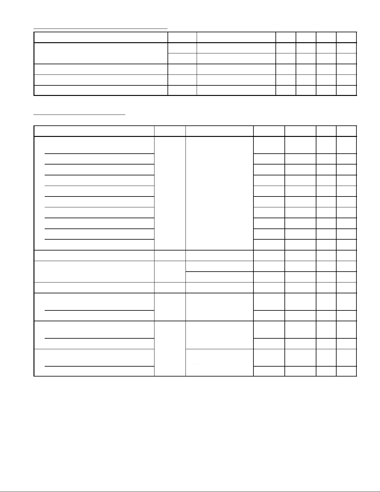
Recommended Operating Conditions:
CC1
Parameter Symbol Test Conditions Min Typ Max Unit
Supply Voltage V
V
CC1
CC2
10.8 12.0 13.2 V
10.0 25.0 35.0 V
Cascade Input Voltage (When not at GND) 1 – 8 V
Output Current I
Operating Ambient Temperature T
O
A
– – 25 mA
0 – 70 °C
Electrical Characteristics: (TA = 0° to +70°C, Pin5 at GND, Pin6 Open, Note 2 unless otherwise
specified)
Parameter Symbol Test Conditions Min Typ Max Unit
Positive–Going Threshold Voltage at Input A
Switching Q1 V
T+
Switching Q2 325 400 475 mV
Switching Q3 525 600 675 mV
Switching Q4 725 800 875 mV
Switching Q5 925 1000 1075 mV
Switching Q6 1 125 1200 1275 mV
Switching Q7 1325 1400 1475 mV
Switching Q8 1525 1600 1675 mV
TA = +25°C 125 200 275 mV
Switching Q9 1725 1800 1875 mV
Switching Q10 1925 2000 2075 mV
Input Hysteresis VT+ – V
High–Level (On–State) Output Voltage V
Low–Level (Off–State) Output Current I
OH
OL
T–
IOH = –10mA V
IOH = –25mA V
V
= 35V – 0.5 200 µA
CC2
– 10 – mV
CC2
CC2
–1.3 V
–1.5 V
–0.8 – V
CC2
–0.9 – V
CC2
Input Current
Analog Input I
L
VI = 2V – 260 400 µA
Cascade Input – 1000 1700 µA
Supply Current from V
All Outputs High I
CC1
CC
V
= 12V, No Load – 15 25 mA
CC1
All Outputs Low – 9 15 mA
Supply Current from V
All Outputs High
All Outputs Low
Note 2. All typical values are at V
CC2
= 12V, V
CC1
V
= 12V,
CC1
V
= 35V, No Load
CC2
= 25V, and TA = +25°C.
CC2
– 15 27 mA
– 1 200 µA
 Loading...