

NTE15042
Integrated Circuit
Digital Tuning System Interface for TV Systems
Description:
The NTE15042 is an integrated circuit in a 16–Lead DIP type package developed to facilitate the
Phase Lock Loop (PLL) digital tuning system interface for TV systems. Since all the peripheral blocks
are incorporated into this device, the number of peripheral parts can be greatly reduced.
Features:
D All–in–One Chip Incorporating the Peripheral Blocks of the PLL System
D Built–In Synchronized Separate for Channel Detecting Circuit
D Externally Controllable Channel Detection Level
D High Current Low–Saturation–Voltage Band Switch Output: V
D Built–In Channel Tuning Voltage: 34V Typ
Absolute Maximum Ratings: (TA = +25°C unless otherwise specified)
Supply Voltage, V
Band Output Current, I
Band Output Applied Voltage, V
Zener Terminal Current, I
Channel Detection Output Applied Voltage, V
Band Input Voltage, V
Video Signal Input Voltage, V
Error Amplifier Input Voltage, V
Error Amplifier Output Current, I
Flyback Pulse Input Voltage, V
Allowable Power Dissipation (TA = +60°C), P
Operating Temperature Range, T
Storage Temperature Range, T
CC1
I
OH
OL
z
OH
CV
AI
AO
. . . . . . . . . . . . . . . . . . . . . . . . . . . . . . . . . . . . . . . . . . . . . . . .
FBP
D
opr
stg
= 0.3V Typ @ IOH = –40mA
O(sat)
–40° to +150°C. . . . . . . . . . . . . . . . . . . . . . . . . . . . . . . . . . . . . . . . . .
–20° to +65°C. . . . . . . . . . . . . . . . . . . . . . . . . . . . . . . . . . . . . . . . .
0 to V
0 to V
V
600mW. . . . . . . . . . . . . . . . . . . . . . . . . . . . . . . . . . . . . .
14.4V. . . . . . . . . . . . . . . . . . . . . . . . . . . . . . . . . . . . . . . . . . . . . . . . . . . . . . . . . . . . .
–60mA. . . . . . . . . . . . . . . . . . . . . . . . . . . . . . . . . . . . . . . . . . . . . . . . . . . . . . . .
–15V. . . . . . . . . . . . . . . . . . . . . . . . . . . . . . . . . . . . . . . . . . . . . . . . . . .
15mA. . . . . . . . . . . . . . . . . . . . . . . . . . . . . . . . . . . . . . . . . . . . . . . . . . . . . . . . .
V
V. . . . . . . . . . . . . . . . . . . . . . . . . . . . . . . . . . . . .
CC1
V. . . . . . . . . . . . . . . . . . . . . . . . . . . . . . . . . . . . . . . . . . . . . . . . . . . . . . .
CC1
0 to 5V. . . . . . . . . . . . . . . . . . . . . . . . . . . . . . . . . . . . . . . . . . . . . . . . . . .
V. . . . . . . . . . . . . . . . . . . . . . . . . . . . . . . . . . . . . . . . . . . . . .
CC1
–5mA. . . . . . . . . . . . . . . . . . . . . . . . . . . . . . . . . . . . . . . . . . . . . . . . .
CC1 VP
Recommended Operating Conditions:
Parameter Symbol Min Typ Max Unit
Supply Voltage V
Band Signal High–Level Input Voltage e
Band Signal Low–Level Input Voltage e
Video Signal Input Voltage eiv (V3) – 2 – V
Flyback Pulse High–Level Input Voltage e
Flyback Pulse Low–Level Input Voltage e
Incoming Current to Pin11 I
CC1
(V1H, V2H) 3.1 – 5.5 V
BIH
(V1L, V2L) 0 – 0.8 V
BIL
(V4H) 5.0 – 8.0 V
FBPH
(V4L) 0 – 0.7 V
FBPL
11
8.1 12.0 13.2 V
5 – 6 mA
P–P
Electrical Characteristics: (TA = +25°C ±3°C, VCC = 12V unless otherwise specified)
Parameter Symbol Test Conditions Min Typ Max Unit
Circuit Current I
Band Input Threshold Voltage V
Band Output Saturation Voltage V
Band Output Leakage Current I
Zener Stabilization Voltage V
Stabilization Voltage Temperature Factor ∆VZ/∆T TA = –20° to +65°C, IZ = 5mA –5 0 +5 mV/°C
Operating Resistance V
Error Amplifier Input Bias Current I
Error Amplifier Minimum Output Voltage V
Error Amplifier Maximum Output Voltage V
Error Amplifier Reference Input Voltage V
Comparator Reference Voltage 1 V
Comparator Reference Voltage 2 V
Channel Detection Output Low–Level
Voltage
Channel Detection Output Leakage
Current
O(sat)IOH
BIAS
AOL
AOHRL
Cref 1
Cref 2
V
I
OH
Error amp output (High) connected
CC
to the band output V
ITH
= –40mA, I11 = 5mA – 0.3 0.7 V
VOL = –15V – – –50 µA
OL
IZ = 5mA 32 34 36 V
Z
IZ = 5mA – 10 25 Ω
Z
RL = 8.2kΩ – 0.2 0.5 V
= 8.2kΩ VZ –1.5 V
Aref
No signal voltage compared with
voltage when signal is input
Signal voltage compared with no
signal voltage
OLIOL
= 1mA – 0.2 0.5 V
VOH = 13.2V – – 5 µA
CC
2.0 6.0 12.0 mA
1.0 2.0 3.0 V
– – 200 nA
Z
1.5 2.0 2.5 V
6.5 7.0 7.5 V
4.5 5.0 5.5 V
– V
Band Output Format:
BIN
1
L L H Z Z Z
H L Z H Z Z
L H Z Z H Z
H H Z Z Z H
Z: High Impedance
Flyback Pulse Input
Channel Det Output
BIN
2
Band Input 1
Band Input 2
Video Input
(Active High)
BAND
1
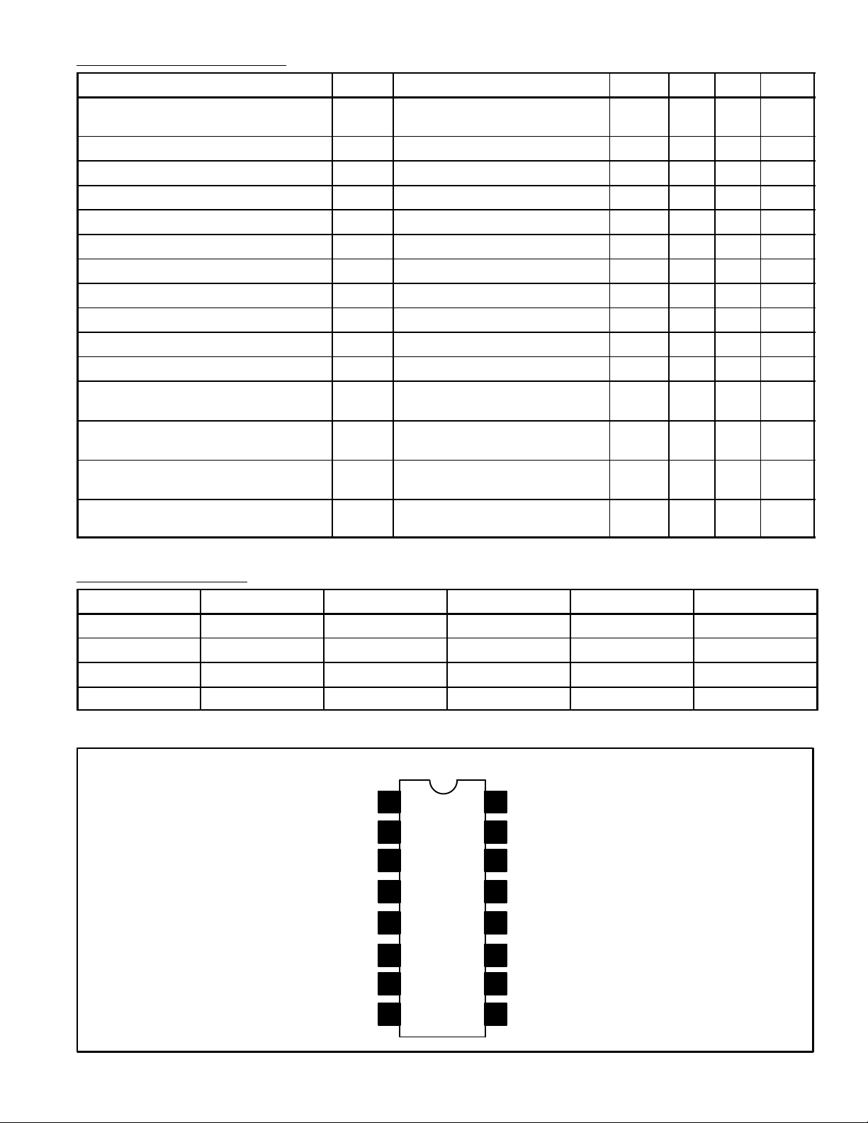
Pin Connection Diagram
1
2
3
4
5GND
6Channel Det Filter
7
BAND
16
15
14
13
12
11
10
2
BAND
Band Output 1
Band Output 2
Band Output 3
Band Output 4
VCC1
VCC2
V
Z
3
BAND
4
8Error Amp Input
Error Amp Output
9
 Loading...