

NTE NTE1501, NTE1500 Datasheet
NTE1500 & NTE1501
Integrated Circuit
7–Step LED Driver Circuit
Description:
The NTE1500 and NTE1501 are integrated circuits designed for driving 7–dot LED displays. The
NTE1500 responds logarithmically to the input signal while the NTE1501 responds linearly. Because
an adjustment pin for output current is provided, the brightness of the LED can be controlled.
Features:
D Linear (NTE1501) and Logarithmic (NTE1500) Response
D 7–LED Bar Graph Display Driver
D Brightness is Externally Adjustable
D High Output Current: 25mA Max
D Series Connection Capable for Driving more than 7–Dot Displays
Absolute Maximum Ratings: (TA = +25°C unless otherwise specified)
Supply Voltage, V
Circuit Voltage, V
Input Voltage, V
Output Voltage, V
Supply Current, I
Output Current, I
Power Dissipation, P
CC
I
I
O
CC
O
D
Operating Ambient Temperature Range, T
Storage Temperature Range, T
stg
opr
–30° to +75°C. . . . . . . . . . . . . . . . . . . . . . . . . . . . . . . . . .
–55° to +150°C. . . . . . . . . . . . . . . . . . . . . . . . . . . . . . . . . . . . . . . . . .
18V. . . . . . . . . . . . . . . . . . . . . . . . . . . . . . . . . . . . . . . . . . . . . . . . . . . . . . . . . . . . . . . .
7.5V. . . . . . . . . . . . . . . . . . . . . . . . . . . . . . . . . . . . . . . . . . . . . . . . . . . . . . . . . . . . . . . . .
16V. . . . . . . . . . . . . . . . . . . . . . . . . . . . . . . . . . . . . . . . . . . . . . . . . . . . . . . . . . . . . . . . . . .
16V. . . . . . . . . . . . . . . . . . . . . . . . . . . . . . . . . . . . . . . . . . . . . . . . . . . . . . . . . . . . . . . . .
25mA. . . . . . . . . . . . . . . . . . . . . . . . . . . . . . . . . . . . . . . . . . . . . . . . . . . . . . . . . . . . . . .
25mA. . . . . . . . . . . . . . . . . . . . . . . . . . . . . . . . . . . . . . . . . . . . . . . . . . . . . . . . . . . . . . . .
1800mW. . . . . . . . . . . . . . . . . . . . . . . . . . . . . . . . . . . . . . . . . . . . . . . . . . . . . . . . .
Electrical Characteristics: (TA = +25°C, VCC = 9V unless otherwise specified)
Parameter Symbol Test Conditions Min Typ Max Unit
Supply Current I
Output Inflow Current I
Reference Voltage V
Output Offset Voltage (Amp) V
Voltage Gain (Amp) G
Output Pin Leakage Current I
(SINK)9–15VI
O(offset)VCC
O(Leak)
tot
REF
V2 = 0 4 – 18 mA
= 3.55V, V7 = 3.5V 13 – 25 mA
3.55 3.75 3.95 V
= 16V, GV = 20dB, V2 = 0 –150 – +150 mV
V2 = 50mV 18 20 22 dB
V
VCC = 18V 0 – 20 µA
Electrical Characteristics (Cont’d): (TA = +25°C, VCC = 9V unless otherwise specified)
Parameter Symbol Test Conditions Min Typ Max Unit
Input Bias Current (Amp) I
Input Bias Current (Comparator) I
Comparator Level (NTE1500) GD1 * V7 = 3.5, V8 = 0 –17 –15 –13 dB
Comparator Level (NTE1501) GD
Bias2
I
Bias3
Bias7
I
Bias1
GD
GD
GD
GD
GD
GD
GD
GD
GD
GD
GD
GD
VCC = 18V, V2 = 0 –2 – 0 µA
VCC = 18V, V3 = 0 –2 – 0 µA
VCC = 18V, V2 = 10V, V3 = 0, V7 = 0 –10 – 0 µA
VCC = 18V, V3 = 10V, VI = 0, V2 = 0,
= V
V
6
7
2
3
4
5
6
7
V7 = 3.65, V8 = 0 0.4 0.5 0.6 dB
1
2
3
4
5
6
7
–10 – 0 µA
–9 –7 –5 dB
–4 –3 –2 dB
–1 0 1 dB
1.5 2.0 2.5 dB
3.5 4.0 4.5 dB
4.5 5.0 5.5 dB
0.85 1.0 1.15 dB
1.35 1.5 1.65 dB
1.85 2.0 2.15 dB
2.35 2.5 2.65 dB
2.85 3.0 3.15 dB
3.35 3.5 3.65 dB
* The comparator reference voltage is 3.5V and 2.0V is 0dB (VCCopr = 5V to 16V).
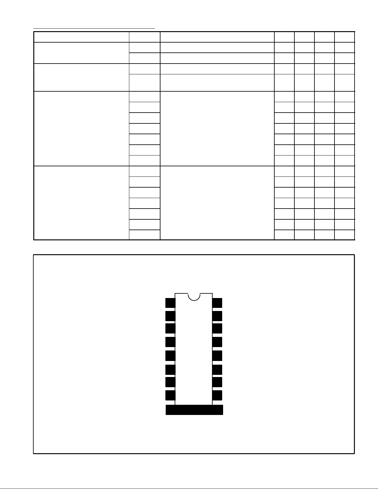
Pin Connection Diagram
Output
Input (–)
Input (+)
LED Current Input
LED Current Input
V
ref
R2
R1
1
2
3
4
5
6
7
8
16
15
14
13
12
11
10
9
V
CC
LED7
LED6
LED5
LED4
LED3
LED2
LED1
GND 17
 Loading...