

NTE NTE1499 Datasheet
NTE1499
Integrated Circuit
1/20 Frequency Divider
Absolute Maximum Ratings: (TA = +25°C unless otherwise specified)
Supply Voltage, V
Supply Current (I
Power Dissipation (T
Operating Temperature Range, T
Storage Temperature Range, T
CC
), I
8
CC
= +70°C), P
A
D
opr
stg
7V. . . . . . . . . . . . . . . . . . . . . . . . . . . . . . . . . . . . . . . . . . . . . . . . . . . . . . . . . . . . . . . . .
20mA. . . . . . . . . . . . . . . . . . . . . . . . . . . . . . . . . . . . . . . . . . . . . . . . . . . . . . . . . . .
140mW. . . . . . . . . . . . . . . . . . . . . . . . . . . . . . . . . . . . . . . . . . . . . .
–20° to +70°C. . . . . . . . . . . . . . . . . . . . . . . . . . . . . . . . . . . . . . . . .
–55°C to +125°C. . . . . . . . . . . . . . . . . . . . . . . . . . . . . . . . . . . . . . . .
Electrical Characteristics:
(TA = +25°C unless otherwise specified)
Parameter Symbol Test Conditions Min Typ Max Unit
Operating Supply Voltage V
CC(opr)
Supply Current I
Input Frequency Range f
Output Voltage Level, “H” V
Output Voltage Level, “L” V
8
i
OH
OL
VCC = 5.2V – 10 13 mA
Sine Wave Input, Vi = 400mV
P–P
VD = 5.2V 4 – – V
IOL = 5mA – – 0.4 V
4.7 5.2 5.7 V
40 – 120 MHz
Minimum Slew Rate SR Rectangular Wave Input – – 100 V/µs
Input Voltage Range V
Sine wave Input 400 – 800 mV
i
P–P
Note 1. The device should be used with Pin5 grounded.
Note 2. The device should be handled with the same precaution as is applied to MOS devices
against electrostatic charge.
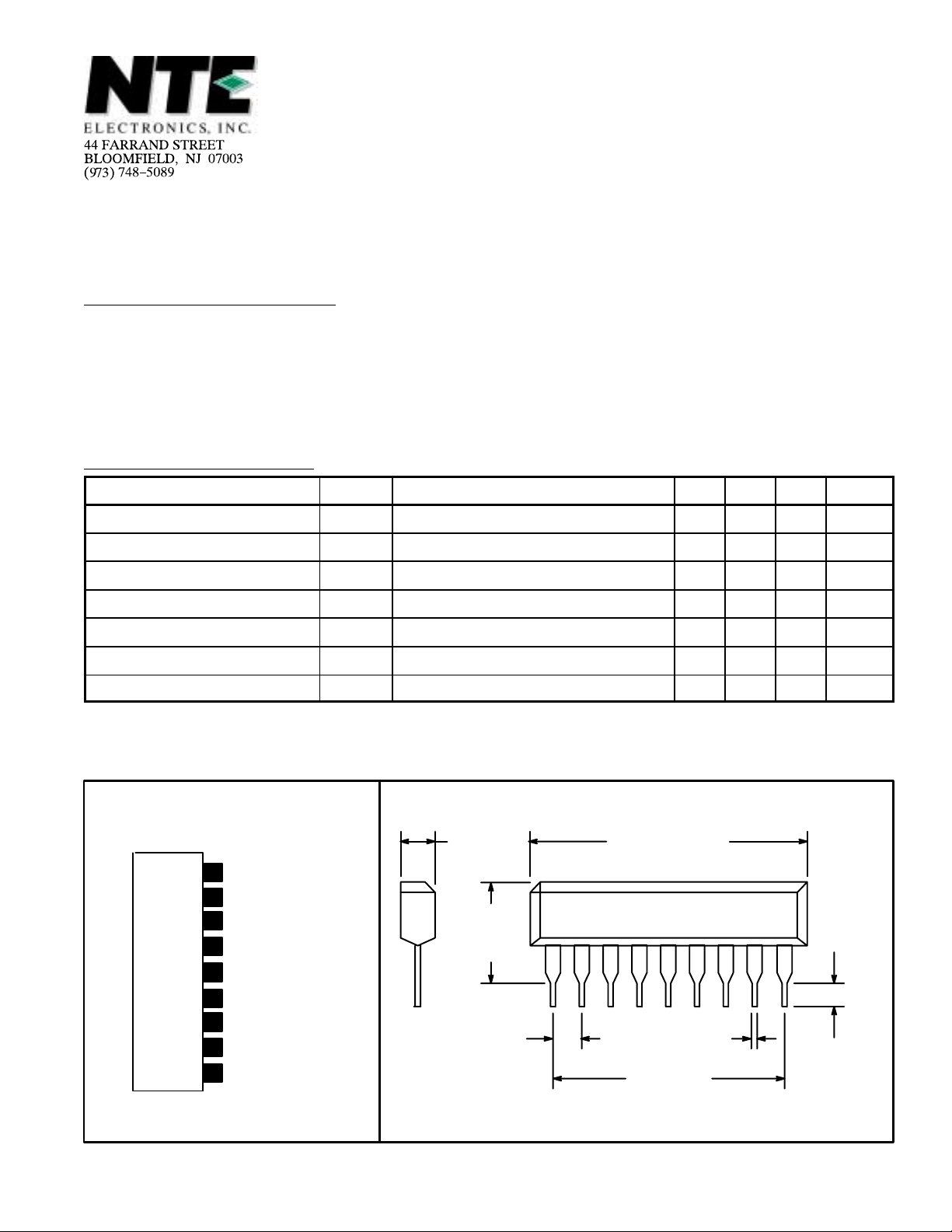
Pin Connection Diagram
(Front View)
Output
9
V
8
CC
Input
7
N.C.
6
GND
5
.323
(8.2)
Max
.906 (23.0) Max.126 (3.2)
19
Filter 1.5nF
4
Filter 1.5nF
3
Filter 1.5nF
2
GND
1
(2.54)
.020 (0.50).100
.800 (20.3)
.099
(2.5)
Min
 Loading...