

NTE NTE1475 Datasheet
NTE1475
Integrated Circuit
CMOS, Phase–Locked Loop (PLL) Frequency
Synthesizer for CB
Features:
D Built–in high speed programmable divider for direct PLL system
D PLL out–of–lock output available to inhibit transmittion.
D Instantaneous call capability of channel 9 and 19.
D Built–in detecting circuit of mis–program
D Built–in amplifier for crystal oscillator
D Built–in amplifier for active low–pass filter.
D BCD code channel selection. (Pull–down resistors included)
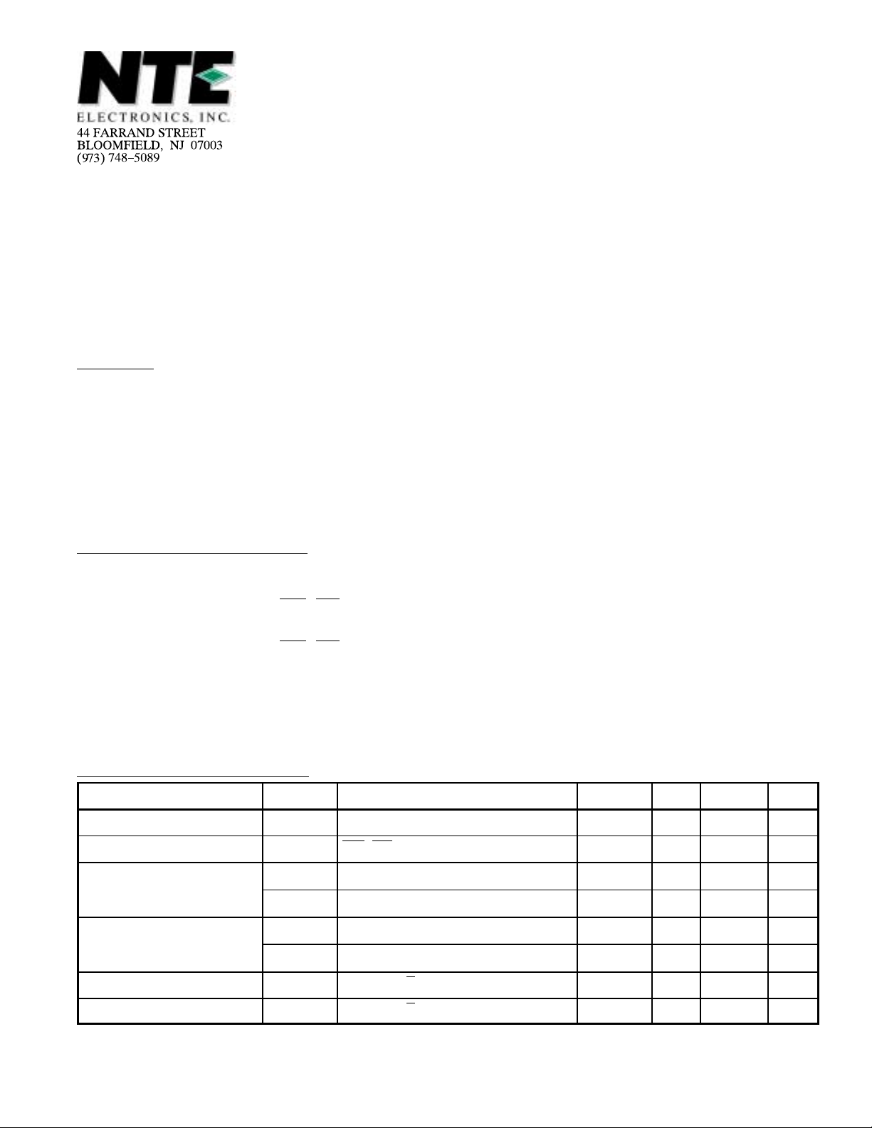
Absolute Maximum Ratings:
Maximum Supply Voltage, V
Maximum Input Voltage, V
Maximum Output Voltage (MC, LM, A
Maximum Output Voltage (PD
Maximum Output Current (MC, LM), I
Maximum Output Current (A
(TA = +25°C unless otherwie specified)
max –0.3 to +8.0V. . . . . . . . . . . . . . . . . . . . . . . . . . . . . . . . . . . . . . . . . .
DD
max –0.3 to VDD +0.3V. . . . . . . . . . . . . . . . . . . . . . . . . . . . . . . . . . . . . . . .
IN
, Output Off), V
OUT
), I
OUT
OUT (2)
, Output Off), V
OUT
OUT (1)
OUT(1)
OUT(2)
–0.3 to +10.0V. . . . . . . . . . . . . . . .
–0.3 to VDD + 0.3V. . . . . . . . . . . . . . . . . . . . .
0 to 2.5mA. . . . . . . . . . . . . . . . . . . . . . . . . . . . . . . . . . . . . . . .
Allowable Power Dissipation, PDmax (TA = +70°C) 300mW. . . . . . . . . . . . . . . . . . . . . . . . . . . . . . . . .
Operating Temperature Range, T
Storage Temperature Range, T
Allowable Operating Ranges
Parameter Symbol Test Conditions Min Typ Max Unit
Supply Voltage V
Output Voltage V
Input Amplitude
Input Frequency
stg
: (TA = +25°C unless otherwise specified)
DD
OUT
V
IN (1)
V
IN (2)
f
IN (1)
f
IN (2)
opg
TA = –30° to +70°C 5.0 6.0 7.0 V
MC, LM, A
XIN, f
IN (1)
PIN, f
IN (2)
XIN, V
IN (1)
PIN, V
IN (2)
, Output Off 0 – 9.0 V
OUT
= 10.25MHZ, Note 1 1.0 – 0.9V
= 20MHZ, Note 1 1.0 – 0.9V
= 1.0V
= 1.0V
, Note 1 1.0 – 10.25 MH
p–p
, Note 1 1.0 – 20 MH
p–p
–30° to +70°C. . . . . . . . . . . . . . . . . . . . . . . . . . . . . . . . . . . . . . . . .
–40° to +125°C. . . . . . . . . . . . . . . . . . . . . . . . . . . . . . . . . . . . . . . . . .
DD
DD
0 to 15mA. . . . . . . . . . . . . . . . . . . . . . . . . . . . . . . . . . . . .
V
p–p
V
p–p
Z
Z
Input “H” Level Voltage V
Input “L” Level Voltage V
IH
IL
D1 to D6, T/R, CH9, CH19 VDD–0.8 – – V
D1 to D6, T/R, CH9, CH19 – – 0.8 V
Note 1. Sinusoidal wave, capacitive coupling, TA = –30° to +70°C
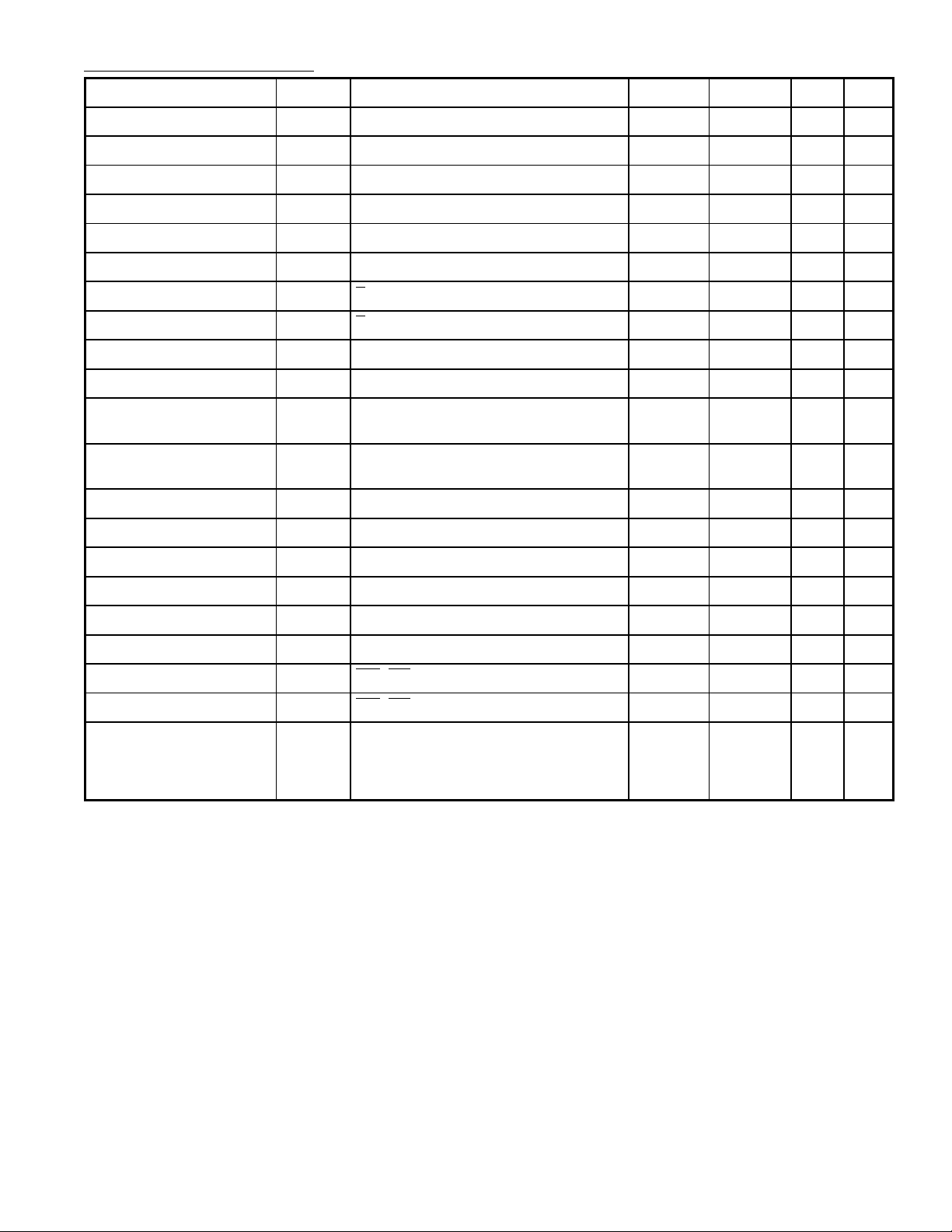
Electrical Characteristics: (TA = +25°C, VDD = 5V to 7V unless otherwise specified)
Parameter Symbol Test Conditions Min Typ Max Unit
Input “H” Level Current I
Input “L” Level Current I
IH (1)
IL (1)
Feedback Resistance R
Input Threshold Voltage V
Input “H” Level Current I
IH (2)
Input Floating Voltage V
Input “L” Level Current I
IL (2)
Input Floating Voltage V
Input “H” Level Current I
Input “L” Level Current I
“H” Level 3–State Leak
IH (3)
IL (3)
I
OFFH
Current
“L” Level 3–State Leak
I
OFFL
Current
Output “H” Level Voltage V
Output “L” Level Voltage V
Output “H” Level Voltage V
Output “L” Level Voltage V
Output “L” Level Voltage V
Output Off Leak Current I
Output “L” Level Voltage V
Output Off Leak Current I
OH (1)
OL (1)
OH (2)XOUT
OL (2)
OL (3)
OFF (1)AOUT
OL (4)
OFF (2)
Current Dissipation I
F
th
IF (1)
IF (2)
DD
XIN, PIN, VIN = V
XIN, PIN, VIN = V
XIN, P
IN
XIN, P
IN
DD
SS
D1 to D6, CH9, CH19, VIN = V
DD
– – 8.0 µA
– – 8.0 µA
– 3.0 – MΩ
– 1/2 V
DD
– V
60 180 500 µA
D1 to D6, CH9, CH19, Input pins open – – 0.2 V
T/R, VIN = V
SS
40 140 400 µA
T/R, Input pin open VDD–0.2 – – V
AIN, VIN = V
AIN, VIN = V
PD
OUT
PD
OUT
PD
OUT
PD
OUT
, I
X
, I
OUT
A
, I
OUT
, V
MC, LM, I
MC, LM, V
f
= 10.25MHZ, f
IN (1)
V
IN (1)
= VSS, D1 = VDD, Other pins open,
A
IN
DD
SS
, V
= V
, V
, I
, I
OUT
OUT
OUT
OUT
= V
OUT
OUT
OUT
OUT
OUT
IN (2)
DD
= V
SS
= 0.3mA VDD–1.0 – – V
= 0.3mA – – 1.0 V
= 0.5mA – VDD–0.35 – V
= 0.5mA – 0.35 – V
= 0.5mA – – 0.3 V
= 9V – – 3.0 µA
= 15mA – – 1.1 V
= 9V – – 5.0 µA
OUT
= 20MHZ,
IN (2)
= 1.0V
p–p
,
– 0.01 – nA
– 0.01 – nA
– 0.01 – nA
– 0.01 – nA
– 10 20 mA
Number of frequency
 Loading...