

NTE NTE1442 Datasheet
NTE1442
Integrated Circuit
Balance Modulator
Features:
D Broad Band (10MHz), Good Carrier Suppression
D Carrier Suppression Within –40dB (10mV
Absolute Maximum Ratings: (TA = +25°C unless otherwise specified)
Supply Voltage (V
Supply Current, I
Power Dissipation, P
Operating Temperature Range, T
Storage Temperature Range, T
8–11
CC
), V
D
CC
opr
stg
Electrical Characteristics: (TA = +25°C unless otherwise specified)
Parameter Symbol Test Conditions Min Typ Max Unit
DC Current Gain hFE (T8) 40 100 300
rms
to 1V
Output Signal)
rms
–20° to +70°C. . . . . . . . . . . . . . . . . . . . . . . . . . . . . . . . . . . . . . . . .
–55° to +150°C. . . . . . . . . . . . . . . . . . . . . . . . . . . . . . . . . . . . . . . . . .
14.4V. . . . . . . . . . . . . . . . . . . . . . . . . . . . . . . . . . . . . . . . . . . . . . . . . . . . . . .
15mA. . . . . . . . . . . . . . . . . . . . . . . . . . . . . . . . . . . . . . . . . . . . . . . . . . . . . . . . . . . . . . .
400mW. . . . . . . . . . . . . . . . . . . . . . . . . . . . . . . . . . . . . . . . . . . . . . . . . . . . . . . . . . .
hFE (T7) 40 100 300
Output Offset Current (1) I8–I
Output Offset Current (2) I8–I
Output Offset Current (3) I8–I
Output Offset Current (4) I8–I
7
7
7
7
–100 0 100 µA
–100 0 100 µA
–100 0 100 µA
–100 0 100 µA
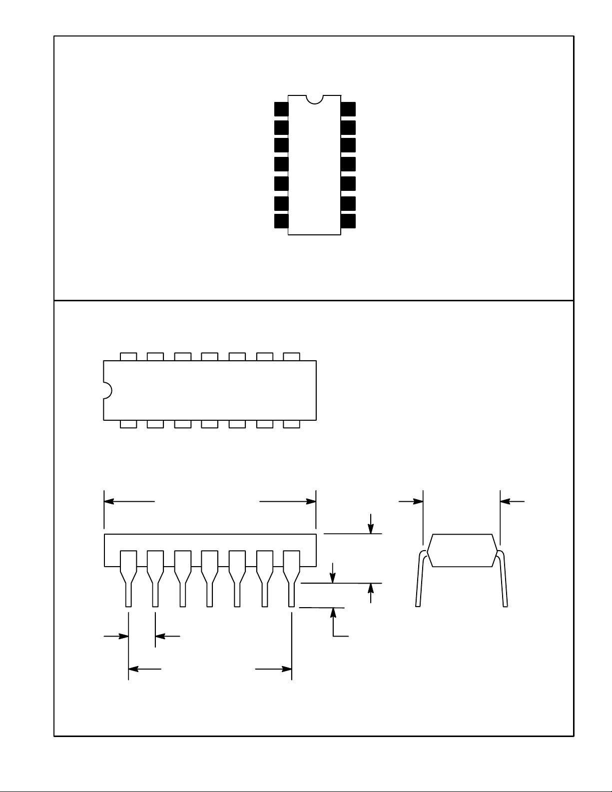
Pin Connection Diagram
560Ω Bias Resistor
2.7k to Pin4
To Pin9
7µF Bypass
1
2
3
4
5Carrier Input
6Carrier Input
CC
7
V
14 8
To Pin9
14
13
1kΩ Resistor
1kΩ Resistor
12
11 Balance
Signal Input
10
9
1kΩ to Pin3
8 Output
17
.785 (19.95) Max
.300 (7.62)
.200
(5.08)
Max
.100 (2.45) .099 (2.5) Min
.600 (15.24)
 Loading...