

NTE NTE1434 Datasheet

NTE1434
Integrated Circuit
Voltage Comparator
Description:
The NTE1434 is an integrated circuit in a 5–Lead SIP type package designed for use as a voltage
comparator that operates from a single power supply.
Features:
D Low Input Current
D Wide Operating Voltage Range
D Low Power Dissipation
D High Output Breakdown Voltage
D Capable of Directly Driving a Relay or a Lamp
Applications:
D Voltage Comparator
D Electric Shutter
D CR Timer
D Time Delay Circuit
D Oscillator (Square Wave)
Absolute Maximum Ratings: (TA = +25°C unless otherwise specified)
Supply Voltage, V
Input Voltage, V
Output Drive Current (Output Saturated), I
Output Drive Voltage, V
Power Dissipation, P
CC
. . . . . . . . . . . . . . . . . . . . . . . . . . . . . . . . . . . . . . . . . . . . . . . . . . . . . . . . . . . . . . . . . .
IN
OL
OH
D
180mW. . . . . . . . . . . . . . . . . . . . . . . . . . . . . . . . . . . . . . . . . . . . . . . . . . . . . . . . . . .
Derate Above 25°C 1.8mW/°C. . . . . . . . . . . . . . . . . . . . . . . . . . . . . . . . . . . . . . . . . . . . . . . . . . . . .
Operating Temperature Range, T
Storage Temperature Range, T
stg
opr
–20° to +75°C. . . . . . . . . . . . . . . . . . . . . . . . . . . . . . . . . . . . . . . . .
–40° to +125°C. . . . . . . . . . . . . . . . . . . . . . . . . . . . . . . . . . . . . . . . . .
Recommended Operating Conditions:
Supply Voltage Range 2.5V to 28V. . . . . . . . . . . . . . . . . . . . . . . . . . . . . . . . . . . . . . . . . . . . . . . . . . . . . . .
Rated Voltage 12V. . . . . . . . . . . . . . . . . . . . . . . . . . . . . . . . . . . . . . . . . . . . . . . . . . . . . . . . . . . . . . . . . . . . .
28V. . . . . . . . . . . . . . . . . . . . . . . . . . . . . . . . . . . . . . . . . . . . . . . . . . . . . . . . . . . . . . . .
V
CC
50mA. . . . . . . . . . . . . . . . . . . . . . . . . . . . . . . . . . . . . . . . .
30V. . . . . . . . . . . . . . . . . . . . . . . . . . . . . . . . . . . . . . . . . . . . . . . . . . . . . . . . . . .
Electrical Characteristics: (TA = +25°C, VCC = 12V unless othrwise specified)
Parameter Symbol Test Conditions Min Typ Max Unit
Supply Voltge Range V
Circuit Current I
Inverting Input Voltage V
Non–Inverting Input Voltage V
Inverting Input Current I
Non–Inverting Input Current I
Input Offset Voltage V
Output Saturation Voltage V
Propagation Delay Time t
t
CC
CC
IN(1)
IN(2)
IN(1)
IN(2)
Reference Voltage at Pin1 –7 +2 +12 mV
IO
OL
VCC = 6V, RL = 100Ω – 0.3 0.6 V
VCC = 12V, RL = 200Ω – 0.3 0.6 V
VCC = 24V, RL = 400Ω – 0.3 0.6 V
PLH
PHL
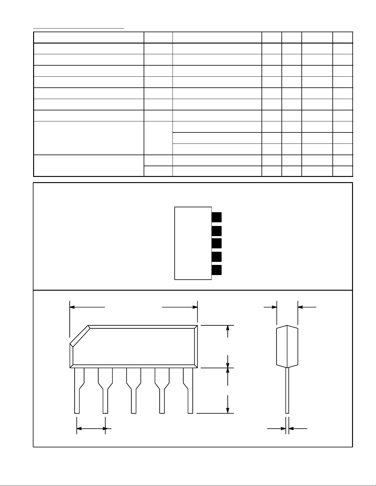
Pin Connection Diagram
(Front View)
5
2.5 – 28 V
– 1.8 2.5 mA
1.4 – VCC–0.2 V
1.4 – VCC–0.2 V
– 20 75 nA
– 20 75 nA
– 1 – µs
– 10 – µs
GND
V
4
CC
Output
3
Non–Invert Input
2
1
Invert Input
.466 (11.8) Max
.078 (1.98) Max
.163
(4.2)
15
.192 (4.8) Min
.100 (2.54) Typ
.013 (0.33)
 Loading...