NTE NTE1414 Datasheet

NTE1414
Integrated Circuit
Digital AC Clock Timer for VCR
Description:
The NTE1414 is an LSI integrated circuit in a 40–Lead DIP type package designed for AC INPUT
clock timers capable of randomly setting “ON hour” and “OFF hour” by a unit of a minute. This device
can also work as a stopwatch timing up to 1 hour, 59 minutes and 59 seconds, and as a sleep timer
operating for not more than 1 hour and 59 minutes once it is set.
A current hour, “ON hour”, and “OFF hour” can be set easily in one of the following three modes: FAST
mode, in which the data of figures of minutes are sent fast at 50Hz or 60Hz; SLOW mode, in which
they are sent slow at 2Hz; and REVERSE, mode in which they are sent reversely.
Features:
D Complete Two–Operation/24 Hour Timer
D Alternate Current of 50Hz/60Hz Entered
D AM/PM or 24 Hour Display
D Hours can be Set in FORWARD or REVERSE Mode
D Sleep Timer Operation for not more than 1 Hour, 59 Minutes once it is Set
D Stopwatch Timing up to 1 Hour, 59 Minutes, and 59 Seconds
D Capable of Directly Driving a Fluorescent Lamp Tube
D Power Failure Indicator
Absolute Maximum Ratings: (VSS = 0, TA = +25°C unless otherwise specified)
Supply Voltage, V
Input Voltage, V
Output Voltage, V
Operating Ambient Temperature Range, T
Storage Temperature Range, T
DD
I
O
opr
stg
Recommended Operating Conditions: (TA = +25°C unless otherwise specified)
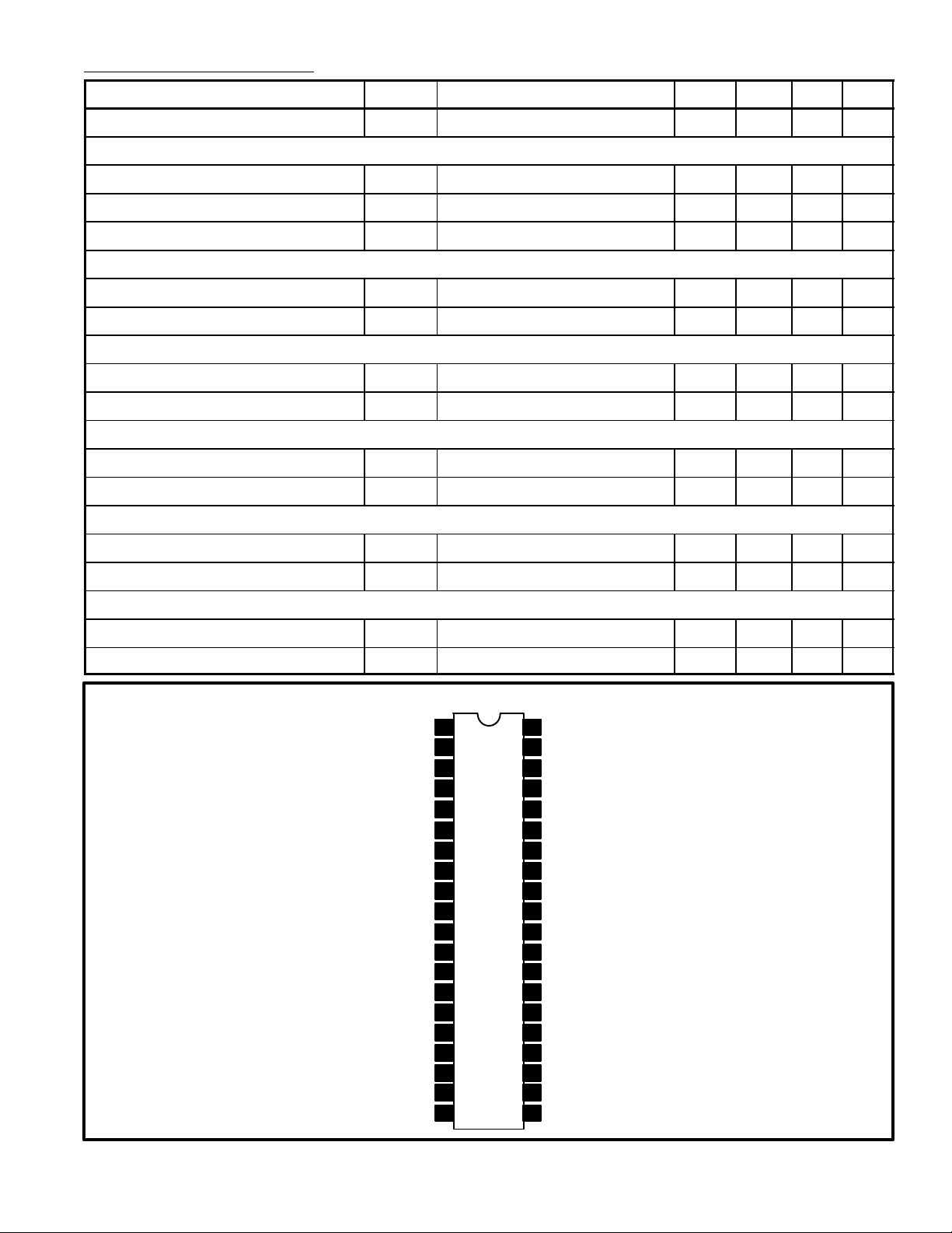
Parameter Symbol Test Conditions Min Typ Max Unit
Supply Voltage V
Supply Voltage Fall Detect Voltage V
DD
VSS = 0 –10 – –15 V
VSS = 0 – – –10 V
PF
–16 to +0.3V. . . . . . . . . . . . . . . . . . . . . . . . . . . . . . . . . . . . . . . . . . . . . . . . . . . . . . . .
–17 to +0.3V. . . . . . . . . . . . . . . . . . . . . . . . . . . . . . . . . . . . . . . . . . . . . . . . . . . . . . . . . . .
–26 to +0.3V. . . . . . . . . . . . . . . . . . . . . . . . . . . . . . . . . . . . . . . . . . . . . . . . . . . . . . . . .
–20° to +70°C. . . . . . . . . . . . . . . . . . . . . . . . . . . . . . . . . .
–40° to +125°C. . . . . . . . . . . . . . . . . . . . . . . . . . . . . . . . . . . . . . . . . .

Electrical Characteristics: (VDD = –12V, VSS = 0, TA = +25°C unless otherwise specified)
Parameter Symbol Test Conditions Min Typ Max Unit
Supply Current I
DD
No Load – 1.3 5.0 mA
50Hz/60Hz Input Terminal
Input Frequency f
High Level Input Voltage V
Low Level Input Voltage V
i
IH (1)
IL (1)
VSS = 0 0 – –1 V
VSS = 0 VDD+1 – –16 V
DC 50/60 10k Hz
All Other Input Terminals
High Level Input Voltage V
Low Level Input Voltage V
IH (2)
IL (2)
VSS = 0 0 – –1 V
VSS = 0 VDD+1 – V
PM Output Terminal (In 24 Hour Display Mode)
High Level Output Current I
OH (
Output Voltage Breakdown BV
O (1)IO
VO = –3V – 12 – mA
1)
= –10µA – – –22 V
10’s of Hour and 10’s of Minute – Figure Display Output Terminal (b & c) (a & d)
High Level Output Current I
OH (2
Output Voltage Breakdown BV
O (2)IO
VO = 3V – 6 – mA
)
= –10µA – – –22 V
Other Display Output Terminals
High Level Output Current I
OH (3
Output Voltage Breakdown BV
O (3)IO
VO = –3V – 3 – mA
)
= –10µA – – –22 V
Other Output Terminals
DD
V
High Level Output Current I
OH (4
Output Voltage Breakdown BV
10 Hrs – b & c
10 Mins – g
10 Mins – a & d
10 Mins – b
10 Mins – e
Mins – g
Mins – a
Mins – b
Mins – e
VO = –2V 500 – – µA
)
O (4)IO
= –10µA – – –22 V
Pin Connection Diagram
AM
Hrs – f
Hrs – g
Hrs – b
Hrs – d
Hrs – c
Hrs – e
1
2
3
4
5Hrs – a
6
7
8
9 32
1010 Mins – f
11
12 29
13
14
1510 Mins – c 26
16Mins – f
17
18 23
19
20 21
40
39
38
37
36
35
34
33
31
30
28
27
25
24
22
PM
1Hz Output
12/24 Select
Blanking
50/60 Select
50/60 Input
Forward/Reverse
Slow
Fast
MS 1
MS 2
MS 3
V
SS
V
DD
Timer OFF Input
Timer ON Input
Timer Output
Timer Output
Mins – c
Mins – a
 Loading...