

NTE NTE1410 Datasheet
NTE1410
Integrated Circuit
Chroma Video Signal Processor
Description:
The NTE1410 is an integrated circuit in a 28–Lead DIP type package designed for all color TV video
and chrominance signal process circuits.
Features:
D The NTE1410 provides a total video and chrominance signal processing circuitry, allowing
compact set design
D Incorporating luminance signal mixing circuit and provides R.G.B. original color output
D All DC control system for simplicity of wiring (color, tint, contrast, picture, luminance)
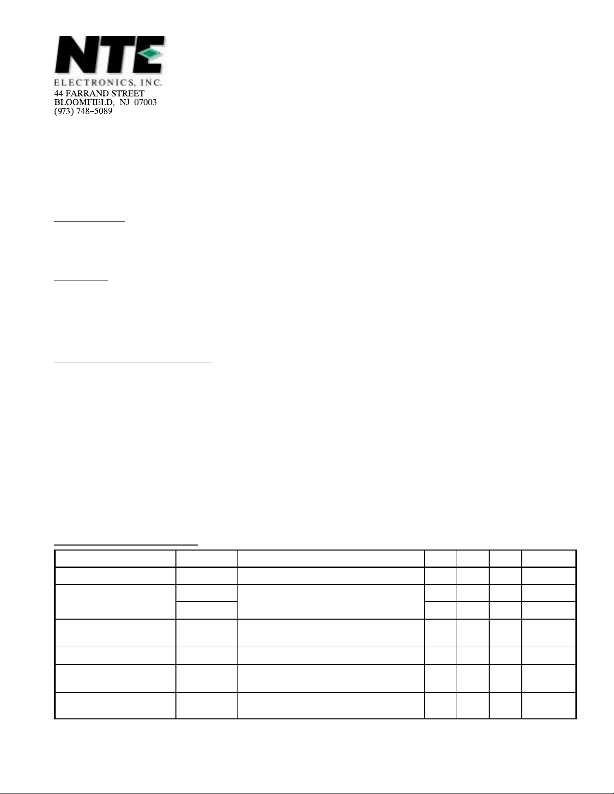
Absolute Maximum Ratings
Supply Voltage, V
CC
: (TA = +25°C unless otherwise specified)
Circuit Voltage
V
1–14
V
3,4,7,8,9,10–14
V
20–14
V
24–14
. . . . . . . . . . . . . . . . . . . . . . . . . . . . . . . . . . . . . . . . . . . . . . . . . . . . . . . . . . . . . . . . . . . . .
. . . . . . . . . . . . . . . . . . . . . . . . . . . . . . . . . . . . . . . . . . . . . . . . . . . . . . . . . . . . . .
Circuit Current, I
Power Dissipation (T
Operating Ambient Temperature Range, T
Storage Temperature Range, T
. . . . . . . . . . . . . . . . . . . . . . . . . . . . . . . . . . . . . . . . . . . . . . . . . . . . . . . . .
, I27, I
26
28
= +70°C), PD 750mW. . . . . . . . . . . . . . . . . . . . . . . . . . . . . . . . . . . . . . . . . . . . . .
A
opr
stg
Note 1. and are flow–in and flow–out currents to/from the circuit, respectively.
Electrical Characteristics
Parameter Symbol Test Conditions Min Typ Max Unit
Total Circuit Current I
Circuit Voltage V
Output Voltage (Burst) V
: (TA = +25°C unless otherwise specified)
tot
11–14
V
26, 27, 28–14
O(1)
VCC = 12V 33 44 56 mA
VCC = 12V 7.5 8.5 9.2 V
Rainbow 150mV
Contrast Max.
, Color AUTO Center,
P–P
3.5 4.0 4.5 V
0.5 0.7 0.9 V
0V to 14.4V. . . . . . . . . . . . . . . . . . . . . . . . . . . . . . . . . . . . . . . . . . . . . . . . . . . . . . . . . . . . . . . .
0V to V
–6V to V
–20° to +70°C. . . . . . . . . . . . . . . . . . . . . . . . . . . . . . . . . .
–40° to +125°C. . . . . . . . . . . . . . . . . . . . . . . . . . . . . . . . . . . . . . . . . .
–40mA. . . . . . . . . . . . . . . . . . . . . . . . . . . . . . . . . . . . . . . . . . . . . . . . . . . . . . . .
14.4V. . . . . . . . . . . . . . . . . . . . . . . . . . . . . . . . . . . . . . . . . . . . . . . . . . . . . . . . . . . . . .
V
P–P
1–14
1–14
1–14
ACC Characteristics ACC Rainbow 15mV
Output Voltage (Chroma) V
Oscillation Frequency f
O(2)
OSC
Rainbow 150mV
Max.
Pin13 Input Invalid Signal, Trimmer to be
Set by Standard Samples, Note 2
Note 2. f: Deviation from 3579545Hz.
, Burst Output/V
P–P
, Color Max., Contrast
P–P
O(1)
0.6 0.8 1.0 times
0.5 0.7 0.9 V
– – ±150 Hz
P–P
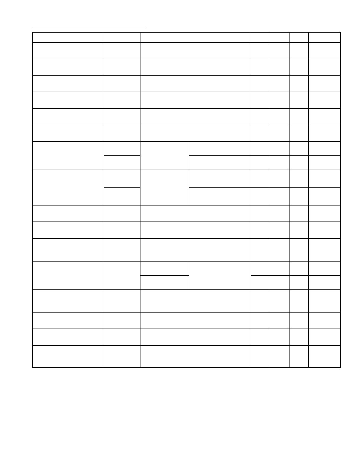
Electrical Characteristics (Cont’d): (TA = +25°C unless otherwise specified)
∠
Parameter Symbol Test Conditions Min Typ Max Unit
f
Drift with
OSC
Supply Voltage
f
Drift with
OSC
Ambient Temperature
Df
OSC/VCC
Df
OSC/TA
Pin16 and pin17 Short–Circuit, VCC = 12V,
Note 3
TA = –20° to +70°C, Pin16 an d P in17 S hort–
Circuit, IC Unit, Note 4
– – ±60 Hz
0 –1 –2 Hz/deg.
Control Sensitivity (VCO) b Burst Input 0.7V
for 100Hz V ariation
Phase Detector Sensitivity m Burst Input 0.7V
Phase Hold
Characteristics
APC Pull–In Range f
Error and V
DF Burst Input 0.7V
Variation
APC
Burst Input 0.7V
16–17
Changed for Measurement
Demodulation Output
Ratio
Ratio
Demodulation Angle
R/B
G/B
∠ R
(1)
(2)
Demodulation
Input 0.2V
Input 0.2V
P–P
P–P
f = 3.59MHz,
Note 5
Demodulation
Input 0.2V
P–P
,
,
,
B = 0 deg.,
∠ G
f = 3.59MHz,
Note 5
Color Difference Output
Voltage (Max)
Total Color Difference
Output Voltage
Color Killer Level e
e
e
O(1)
O(2)
K
Demodulator Input 1.2VP, f = 3.5 9 M H z, B R
Output, Note 5
Rainbow 150mV
Contrast Max., R Output, Note 6
Attenuation of Pin13 Input Burst Voltage at
Killer Operating (Burst Voltage 150mV =
0dB), Note 6
, Calculation with V
P–P
, Calculation with Phase
P–P
16–17
1.2 1.5 2.0 Hz/mV
25 45 55 mV/deg.
for 100Hz Change
, Phase Error for 100Hz
P–P
, Burst Frequency to be
P–P
R Output/e
G Output/e
0
0
– 1.5 2.5 deg/100Hz
±450 ±600 – Hz
0.86 0.94 1.04 times
0.25 0.30 0.35 times
R–B Phase Difference 94.0 97.5 102 deg.
G–B Phase Difference 228 235 242 deg.
4.8 5.7 – V
, AUTO Color Center,
P–P
1.28 1.70 2.13 V
–27 –32 –40 dB
P–P
P–P
Voltage Amplification
(Video)
(Video)
Frequency Characteristics
(Video)
A
V
Note 2
f
C
Sine Wave 0.1mV
cy in which A
Studio Color Bar White
Level 1V
Level 1V
, Contrast
, Contrast
P–P
P–P
Max., Picture Min.,
Note 7
Input, Input Frequen-
rms
becomes –6dB, Picture
V1
4.5 5.0 5.5 times
4.6 5.1 5.6 times
5 6 – MHz
Min., B Output, Note 6
DC Transfer Rate T
DC
Video Input, 1V
(Stair–Step),
P–P
68 75 82 %
APL 10 to 90%, B Output
Original Color Output
Voltage (Max.)
Differential Gain DB Video Input 1V
E
O
Output Voltage of each R, G, and B
at V
= 1.2V
3
(Stair–Step, 3.58MHz),
P–P
7.0 – – V
– – 5.0 %
APL 50%, Contrast Max., Picture Max.,
Note 7
Note 2. f: Deviation from 3579545Hz.
Note 3. Max. Width of Variation.
Note 4. Max. Width of Variation 90°C.
Note 5. A
Note 6. V
= 3.5V, Brightness VR Setting, No Blanking.
24
= 3.5V, Brightness VR Setting.
26
Note 7. Outputs of each R, G, and B, Pin26: Pedestal 2V, Brightness VR Setting.
 Loading...