

NTE NTE1408 Datasheet
NTE1408
Integrated Circuit
CMOS, Color Signal Processor for VCR
Description:
The NTE1408 is a CMOS circuit in a 16–Lead DIP type package designed for use in VTR color signal
processing circuitry for the VHS system video tape recorders. This device provides 4 color control
signals, each having 90–degree phase shift.
Absolute Maximum Ratings
Supply Voltage, V
Input Voltage, V
Output Voltage, V
DD
I
O
Operating Temperature Range, T
Storage Temperature Range, T
Electrical Characteristics
: (TA = +25°C unless otherwise specified)
opr
stg
: (f
= 2.52MHz, VCC = 6.2V, VSS = 0V, TA = +25°C unless otherwise
i(FCI)
–0.3V to +8V. . . . . . . . . . . . . . . . . . . . . . . . . . . . . . . . . . . . . . . . . . . . . . . . . . . . . . . .
–0.3V to VDD +0.3V. . . . . . . . . . . . . . . . . . . . . . . . . . . . . . . . . . . . . . . . . . . . . . . . . . . . .
–0.3V to VDD +0.3. . . . . . . . . . . . . . . . . . . . . . . . . . . . . . . . . . . . . . . . . . . . . . . . . . . .
–10° to +70°C. . . . . . . . . . . . . . . . . . . . . . . . . . . . . . . . . . . . . . . . .
–40° to +100°C. . . . . . . . . . . . . . . . . . . . . . . . . . . . . . . . . . . . . . . . . .
specified)
Parameter Symbol Test Conditions Min Typ Max Unit
Supply Current I
Power Dissipation P
Input Terminal FCI
Input Voltage
Pulse Width Duty Ratio tw (duty) 40 50 60 %
Input Terminal SYNC
High Level Input Voltage
Low Level Input Voltage V
Output Leakage Current I
Input Terminal PGI, HDI, IDI, DOC
High Level Input Voltage
Low Level Input Voltage V
Output Leakage Current I
Input Terminal MMI
High level Input Voltage
Low Level Input Voltage V
Output Leakage Current I
Low Level Input Current I
DD
V
V
IH(1)
IL(1)
Leak(1)VI
V
IH(2)
IL(2)
Leak(2)VI
V
IH(3)
IL(3)
Leak(3)VI
No Load, VI = 1.0V
tot
I
= 0V – – –30 µA
= 0V, 6.2V – – ±30 µA
= 1.5V, MMO = “H” – – ±10 µA
VI = 1.5V, MMO = “L” 0.6 1.0 – mA
IL
P–P
– – 1.2 mA
– – 7.44 mW
1.0 – – V
4.6 – 6.2 V
0 – 1.6 V
4.6 – 6.2 V
0 – 1.6 V
4.6 – 6.2 V
– – 1.6 V
P–P
Electrical Characteristics (Cont’d): (f
Parameter Symbol Test Conditions Min Typ Max Unit
Output Terminal FSO
High Level Output Current
Low Level Output Current I
Output Leakage Current I
Output Terminal HSS
High Level Output Current
Low Level Output Current I
Output Leakage Current I
Delay Time t
Output Terminal HDO
Low level Output Current
Output Leakage Current I
Delay Time t
Output Terminal FH0, FH7, MMO
High Level Output Current
Low Level Output Current I
Output Leakage Current I
= 2.52MHz, VCC = 6.2V, VSS = 0V, TA = +25°C unless
i(FCI)
otherwise specified)
I
OH(1)
OL(1)
Leak(4)VO
I
OH(2)
OL(2)
Leak(5)VO
pd(1)
I
OL(3)
Leak(6)VO
pd(2)
I
OH(3)
OL(4)
Leak(7)VO
VO = 4.7V –1.0 –1.5 – mA
VO = 1.5V 1.0 1.5 – mA
= 0, 6.2V – – ±30 µA
VO = 4.7V 1.0 –1.5 – mA
VO = 1.5V 1.0 1.5 – mA
= 0V, 6.2V – – ±30 µA
With Respect to SYNC – – 500 ns
VO = 1.5V 2 3 – mA
= 12V – – 30 µA
With Respect to SYNC – – 500 ns
VO = 4.7V –0.5 –0.75 – mA
VO = 1.5V 0.5 0.75 – mA
= 0V, 6.2V – – ±30 µA
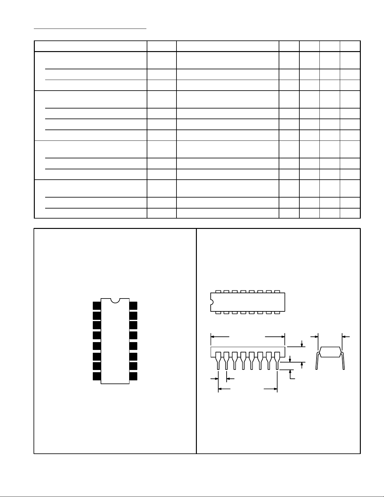
Pin Connection Diagram
V
DD
FH0
V
SS
FSO
IDI
FCI
PGI
HDI
1
2
3
4
5
6
7
8
16
15
14
13
12
11
10
9
FH7
HSS
HDO
MMO
MMI
DOC
SYNC
CNP
16 9
18
.260
.870 (22.0)
Max
.100 (2.54)
.700 (17.78)
.200 (5.08)
Max
.099 (2.5) Min
(6.6)
Max
 Loading...