NTE NTE1396 Datasheet

NTE1396
Integrated Circuit
20W Bridge Booster for Car Radio
Description:
The NTE1396 is a Class B dual audio power amplifier specifically designed for car radio applications.
Power booster amplifiers are easily designed using this device that provides a high current capability
(up to 3.5A) and that can drive very low impedance loads obtaining an output power of more than 20W.
The NTE1396 has high reliability and guarantees complete safety during operation due to protection
against:
D Output DC and AC Short Circuit to GND or Across the Head
D Overrating Chip Temperature (+150°C)
D Polarity Inversion
D Load Dump Voltage Surge
D Fortuitous Open GND
D Very Inductive Loads
Absolute Maximum Ratings:
Operating Supply Voltage, V
DC Supply Voltage, V
S
Peak Supply Voltage (for 50ms), V
Output Peak Current (Note 1), I
S
S
O
Non–Repetitive (t = 0.1ms) 4.5A. . . . . . . . . . . . . . . . . . . . . . . . . . . . . . . . . . . . . . . . . . . . . . . . . . .
Repetitive (f > 10Hz) 3.5A. . . . . . . . . . . . . . . . . . . . . . . . . . . . . . . . . . . . . . . . . . . . . . . . . . . . . . . . .
Power Dissipation (TC = +60°C), P
Operating Junction Temperature Range, T
Storage Temperature Range, T
tot
J
stg
Maximum Thermal Resistance, Junction–to–Case, R
–40° to +150°C. . . . . . . . . . . . . . . . . . . . . . . . . . . . . . . . . .
–40° to +150°C. . . . . . . . . . . . . . . . . . . . . . . . . . . . . . . . . . . . . . . . . .
thJC
18V. . . . . . . . . . . . . . . . . . . . . . . . . . . . . . . . . . . . . . . . . . . . . . . . . . . . . . . .
28V. . . . . . . . . . . . . . . . . . . . . . . . . . . . . . . . . . . . . . . . . . . . . . . . . . . . . . . . . . . . . .
40V. . . . . . . . . . . . . . . . . . . . . . . . . . . . . . . . . . . . . . . . . . . . . . . . . .
30W. . . . . . . . . . . . . . . . . . . . . . . . . . . . . . . . . . . . . . . . . . . . . . . . .
3°C/W. . . . . . . . . . . . . . . . . . . . . . . . . . . . . .
Note 1. Max output current is internally limited.

Electrical Characteristics: (TA = +25°C, Gv = 50dB, R
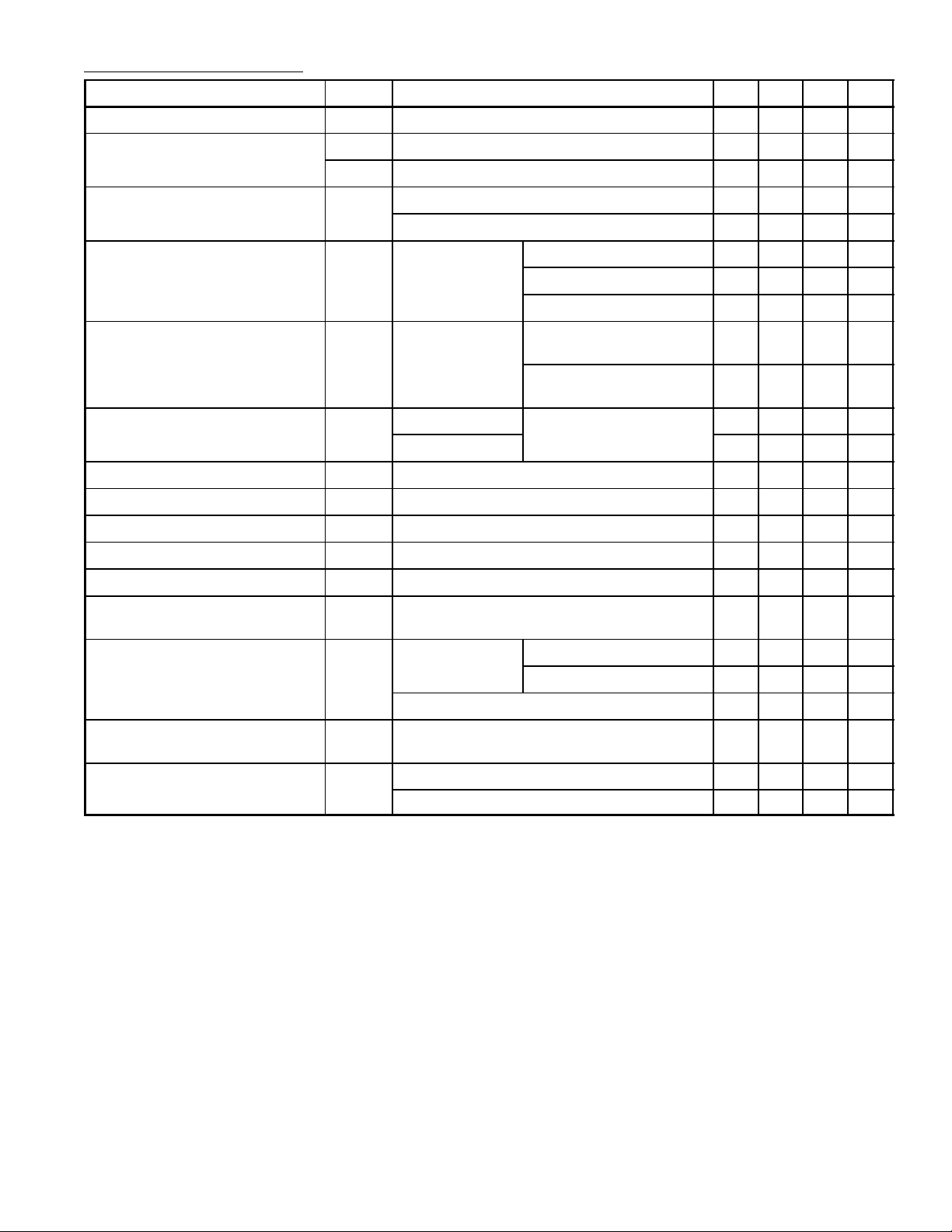
Parameter Symbol Test Conditions Min Typ Max Unit
= 4°C/W, unless oth erwise specified)
th(HS)
Supply Voltage V
Output Offset Voltage
(Between Pin8 & Pin10)
Total Quiescent Drain Current I
S
V
VS = 14.4V – – 150 mV
OS
VS = 13.2V – – 150 mV
VS = 14.4V, RL = 4Ω – 75 150 mA
d
VS = 13.2V, RL = 3.2Ω – 70 160 mA
Output Power P
O
d = 10%,
f = 1kHz
VS = 14.4V, RL = 4Ω 18 20 – W
VS = 14.4V, RL = 3.2Ω 20 22 – W
VS = 13.2V, RL = 3.2Ω 17 19 – W
Distortion d
f = 1kHz VS = 14.4V, RL = 4Ω,
PO = 50mW to 15W
VS = 13.2V, RL = 3.2Ω,
PO = 50mW to 13W
Input Sensitivity V
RL = 4Ω f = 1kHz, PO = 2W – 9 – mV
i
RL = 3.2Ω – 8 – mV
Input Resistance R
Low Frequency Roll Off (–3.2Ω) f
High Frequency f
Closed Loop Voltage Gain G
Total Input Noise Voltage e
f = 1kHz 70 – – kΩ
i
RL = 3.2Ω – – 40 Hz
L
RL = 3.2Ω 20 – – kHz
H
f = 1kHz – 50 – dB
v
Rg = 10KΩ, Note 2 – 3 10 µV
N
Supply Voltage Rejection SVR Rg = 10KΩ , C4 = 10µF, f
V
= 0.5V
ripple
Efficiency η VS = 14.4V ,
f = 1kHz
PO = 20W, RL = 4Ω – 60 – %
PO = 22W, RL = 3.2Ω – 60 – %
ripple
= 100Hz,
8 – 18 V
– – 1 %
– – 1 %
45 55 – dB
VS = 13.2V, f = 1kHz, PO = 19W, RL = 3. 2Ω – 58 – %
Thermal Shut–Down Case
T
VS = 14.4V, RL = 4Ω, f = 1kHz, P
sd
Temperature
Output Voltage with One Side of
the Speaker Shorted to GND
V
OSH
VS = 14.4V, RL = 4Ω – – 2 V
VS = 13.2V, RL = 3.2V – – 2 V
Note 2. Bandwidth filter 22Hz to 22kHz
= 13W 100 110 – °C
tot
 Loading...