

NTE NTE1393, NTE1392 Datasheet
NTE1392 & NTE1393
Integrated Circuit
Audio Power Amp, 7W
Description:
The NTE1392 and NTE1393 are class B power amplifiers in a 10–Lead SIP type package designed
especially for home tpe stereo amplifiers. These devices provide an output power of 5W at 19V, and
also 7W at 22V to an 8Ω load with 10% distortion.
Features:
D Available in Two Different Pin Configurations:
Normal – NTE1392
Reverse – NTE1393
D High Output Power: 7W Typ (VCC = 22V, RL = 8Ω, THD = 10%)
D Wide Range of Supply Voltage: 5V to 30V
D Very Low Harmonic and Crossover Distortion
D Thermal Shut–Down Circuit Provided
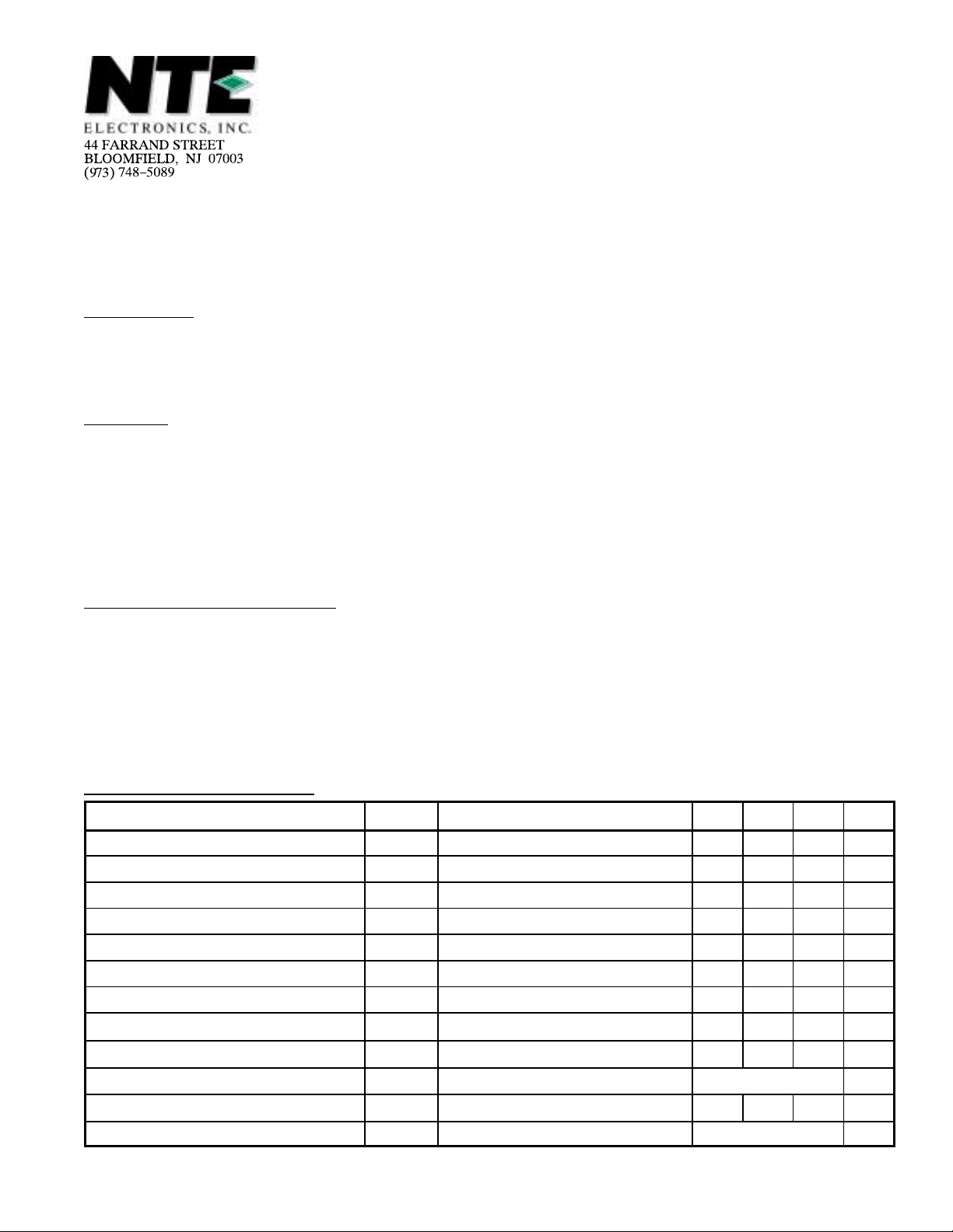
Absolute Maximum Ratings:
Supply Voltage, V
Output Current, I
Power Dissipation (T
CC
O
= +78°C), P
C
Operating Junction Temperature, T
Operating Temperature Range, T
Storage Temperature Range, T
(TA = +25°C unless otherwise specified)
T
J
opr
stg
Thermal Resistance, Junction–to–Case, R
Electrical Characteristics:
Parameter Symbol Test Conditions Min Typ Max Unit
Quiescent Output Voltage V
Quiescent Current Drain I
Input Bias Current I
Output Power P
Total Harmonic Distortion THD P
Voltage Gain (Open Loop) G
Voltage Gain (Closed Loop) G
Noise Output WBN
Input Resistance R
Frequency Response (–3dB) BW C
Supply Voltage Rejection Ratio SVR
Power Band Width (–3dB) PBW C
(TA = +25°C, VCC = 22V, RL = 8Ω unless otherwise specified)
Q
Q
B
OUT
V(OL)
V
in
3.75A. . . . . . . . . . . . . . . . . . . . . . . . . . . . . . . . . . . . . . . . . . . . . . . . . . . . . . . . . . . . . . . .
+150°C. . . . . . . . . . . . . . . . . . . . . . . . . . . . . . . . . . . . . . . . . . . . . . .
–20° to +70°C. . . . . . . . . . . . . . . . . . . . . . . . . . . . . . . . . . . . . . . . .
–55° to +125°C. . . . . . . . . . . . . . . . . . . . . . . . . . . . . . . . . . . . . . . . . .
thJC
10 11 12 V
– 9 20 mA
– 1 – µA
THD = 10&, f = 1kHz 5.8 7.0 – W
= 0.5W, f = 1kHz – 0.06 0.8 %
OUT
f = 1kHz – 75 – dB
f = 1kHz 39 42 45 dB
Rg = 10kΩ, f = 20Hz to 20kHz
f = 1kHz – 100 –
= 330pF, ∆GV = –3dB 60 to 30k Hz
106
f
= 100Hz, Rg = 600Ω
ripple
= 330pF 40 to 70k Hz
106
– 0.3 1.5 mV
38 45 – dB
10°C/W. . . . . . . . . . . . . . . . . . . . . . . . . . . . . . . . . . . . .
30V. . . . . . . . . . . . . . . . . . . . . . . . . . . . . . . . . . . . . . . . . . . . . . . . . . . . . . . . . . . . . . . .
7.2W. . . . . . . . . . . . . . . . . . . . . . . . . . . . . . . . . . . . . . . . . . . . . . . . .
kΩ
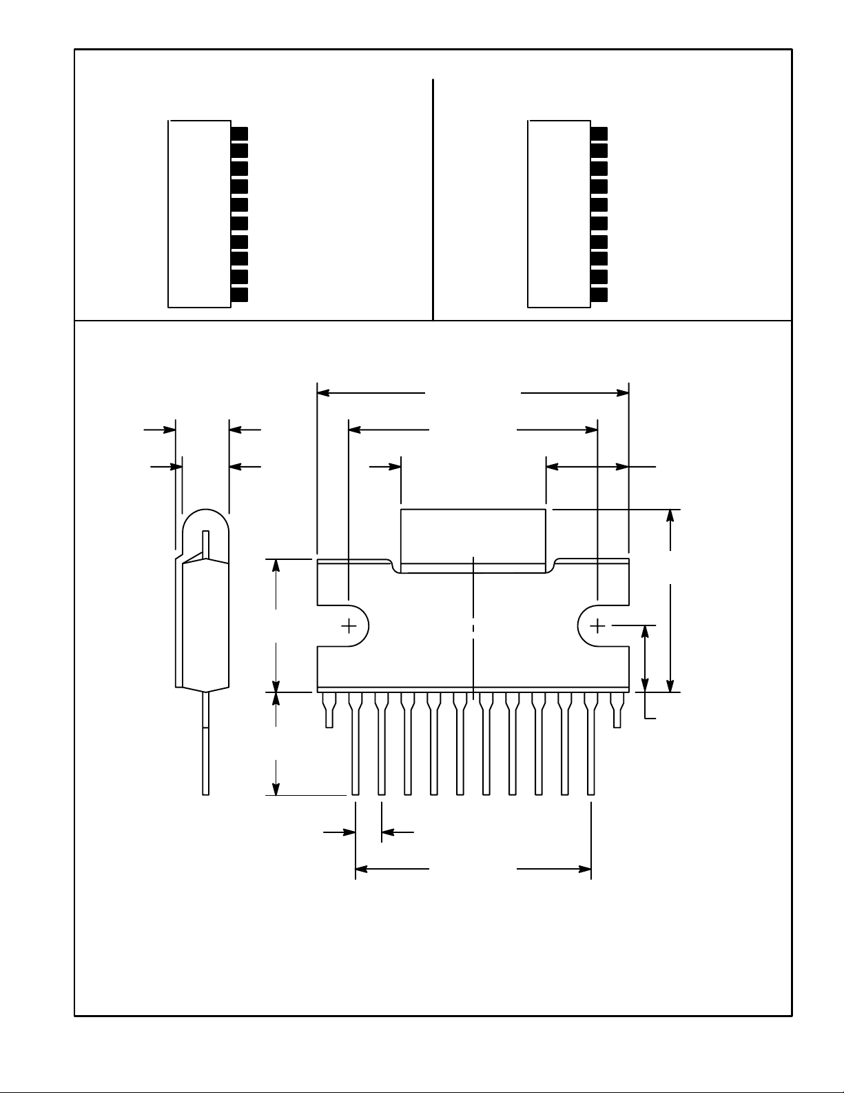
NTE1392
(Front View)
Pin Connection Diagram
NTE1393
(Front View)
10
Feedback
Input
9
Compensation
8
Compensation
7
6
Feedback
5
V
CC
4
Internal Bias
Internal Bias
3
Output
2
GND
1
.150
(3.81)
.120
(3.04)
1.180 (29.97)
.950 (21.13)
1
Feedback
Input
2
Compensation
3
Compensation
4
5
Feedback
6
V
CC
7
Internal Bias
8
Internal Bias
Output
9
GND
10
.320 (8.12).550 (13.97)
.400
(10.16)
.360
(9.14)
.570
(14.47)
110
.270
(6.85)
.100 (2.54)
.900 (22.86)
NOTE: Pin1 and Pin10 are reversed for NTE1393
 Loading...