

NTE NTE1383 Datasheet
NTE1383
Integrated Circuit
Dual Audio Power Amp, 5.1W/Ch
(10.5W BTL)
Description:
The NTE1383 is an integrated circuit in an 18–Lead DIP designed for use as an audio output with low
noise, low distortion, and high output for a wide range of power supply voltages and load resistance.
Two built–in amplifiers provide dual or BTL operation. Typical applications include radio cassette recorder, tape recorder, car stereo, and home entertainment.
Features:
D High Output Power, Dual or BTL Circuit Operation
D Wide Output Power Setting Range
D Wide Supply Voltage Range
D Incorporates an Automatic Operating Point Stabilizer Circuit
D Low Distortion, Low 1/f Noise, and Low Shock Noise
D High Audio Channel Separation
D Incorporates a Phase Converter
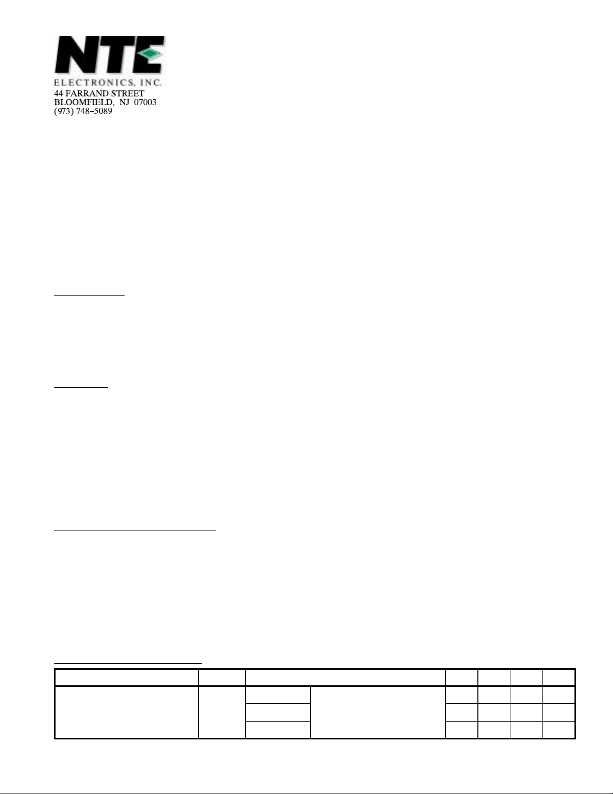
Absolute Maximum Ratings:
Supply Voltage (Note 1), V
Supply Current, I
Power Dissipation (T
CC
= +60°C), P
A
(TA = +25°C unless otherwise specified)
CC
D
Oprating Ambient Temperature Range, T
Storage Temperature Range, T
Note 1. V
at operation mode = 20V (Stabilized power source).
CC
Electrical Characteristics:
Parameter Symbol Test Conditions Min Typ Max Unit
Quiescent Circuit Current I
stg
(TA = +25°C unless otherwise specified)
CQ
VCC = 9V Vi = 0 20 35 55 mA
VCC = 12V
VCC = 13.2V
opr
20V. . . . . . . . . . . . . . . . . . . . . . . . . . . . . . . . . . . . . . . . . . . . . . . . . . . . . . . .
4A. . . . . . . . . . . . . . . . . . . . . . . . . . . . . . . . . . . . . . . . . . . . . . . . . . . . . . . . . . . . . . . . . .
14W. . . . . . . . . . . . . . . . . . . . . . . . . . . . . . . . . . . . . . . . . . . . . . . . .
–30° to +75°C. . . . . . . . . . . . . . . . . . . . . . . . . . . . . . . . . . .
–55° to +150°C. . . . . . . . . . . . . . . . . . . . . . . . . . . . . . . . . . . . . . . . . .
21 40 65 mA
22 40 66 mA
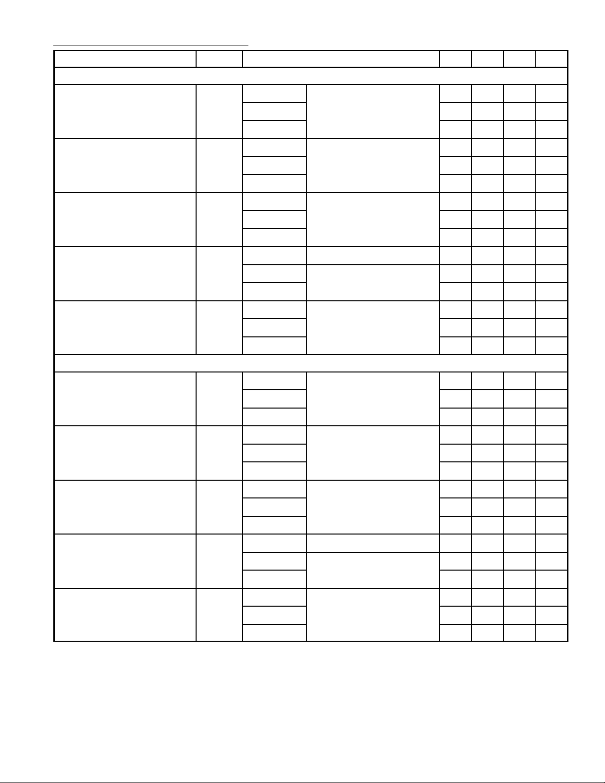
Electrical Characteristics (Cont’d): (TA = +25°C unless otherwise specified)
Parameter Symbol Test Conditions Min Typ Max Unit
BTL (RL = 8Ω, f = 1kHz)
Voltage Gain G
V
Total Harmonic Distortion THD
Output Power P
Output Noise Voltage V
Output Offset Voltage V
O
no
O(offset)
Dual (RL = 4Ω, f = 1kHz)
VCC = 9V
VCC = 12V
VCC = 13.2V
VCC = 9V
VCC = 12V
VCC = 13.2V
VCC = 9V
VCC = 12V
VCC = 13.2V
VCC = 9V
VCC = 12V
VCC = 13.2V
VCC = 9V
VCC = 12V
VCC = 13.2V
Vi = 4mV 40 43 46 dB
40 43 46 dB
40 43 46 dB
Vi = 4mV – 0.15 1.0 %
– 0.15 1.0 %
– 0.15 1.0 %
THD = 10% 4.5 5.0 – W
8.0 9.0 – W
9.4 10.5 – W
Vi = 0, Rg = 3.9kΩ – 0.3 1.0 mV
Vi = 0, Rg = 10kΩ – 0.5 2.0 mV
– 0.7 2.0 mV
Vi = 0 –10 – +10 mV
–12 – +12 mV
–12 – +12 mV
Voltage Gain G
V
Total Harmonic Distortion THD
Output Power P
Output Noise Voltage V
O
no
Channel Balance CB
VCC = 9V
VCC = 12V
VCC = 13.2V
VCC = 9V
VCC = 12V
VCC = 13.2V
VCC = 9V
VCC = 12V
VCC = 13.2V
VCC = 9V
VCC = 12V
VCC = 13.2V
VCC = 9V
VCC = 12V
VCC = 13.2V
Vi = 4mV 41 44 47 dB
42 45 48 dB
42 45 48 dB
Vi = 4mV – 0.3 1.0 %
– 0.3 1.0 %
– 0.3 1.0 %
THD = 10% 2.0 2.4 – W
3.6 4.2 – W
4.5 5.1 – W
Vi = 0, Rg = 3.9kΩ – 0.2 1.0 mV
Vi = 0, Rg = 10kΩ – 0.3 1.5 mV
– 0.3 1.5 mV
Vi = 4mV – 0 1 dB
– 0 1 dB
– 0 1 dB
 Loading...