

NTE NTE1378 Datasheet
NTE1378
Integrated Circuit
Audio Power Amplifier, 10W
Description:
The NTE1378 is a monolithic integrated circuit in a 5–Lead TO220 type package intended for use as
an audio class AB amplifier. Typically , it provides 12W output power (THD = 10%) at V
This device provides high output current and has very low harmonic and cross–over distortion. Further, the NTE1378 incorporates a short circuit protection system comprising an arrangement for automatically limiting the dissipated power so as to keep the working point of the output transistors within
their safe operating area. A thermal shut–down system is also included.
Absolute Maximum Ratings:
Supply Voltage, V
Input Voltage, V
Differential Input Voltage, V
Output Peak Current (Internally Limited), I
Power Dissipation (T
Operating Junction Temperature Range, T
Storage Temperature Range, T
Thermal Resistance, Junction–to–Case, R
Min. Thermal Shut–Down Junction Temperature (V
S
. . . . . . . . . . . . . . . . . . . . . . . . . . . . . . . . . . . . . . . . . . . . . . . . . . . . . . . . . . . . . . . . . . . .
I
I
O
= +90°C), P
C
stg
tot
J
thJC
= ±12V, P
S
= 9W, TA = +25°C), T
tot
= ±12V/4Ω.
S
–40° to +150°C. . . . . . . . . . . . . . . . . . . . . . . . . . . . . . . . . .
–40° to +150°C. . . . . . . . . . . . . . . . . . . . . . . . . . . . . . . . . . . . . . . . . .
sd
±15V. . . . . . . . . . . . . . . . . . . . . . . . . . . . . . . . . . . . . . . . . . . . . . . . . . . . . . . . . . . . . . . .
V
±12V. . . . . . . . . . . . . . . . . . . . . . . . . . . . . . . . . . . . . . . . . . . . . . . . . . . . . . . .
3A. . . . . . . . . . . . . . . . . . . . . . . . . . . . . . . . . . . . . . . . . . . . .
20W. . . . . . . . . . . . . . . . . . . . . . . . . . . . . . . . . . . . . . . . . . . . . . . . .
3°C/W. . . . . . . . . . . . . . . . . . . . . . . . . . . . . . . . . . . . . . .
+110°C.
S
Electrical Characteristics:
Parameter Symbol Test Conditions Min Typ Max Unit
Supply Voltage V
Quiescent Drain Current I
Input Bias Current I
Input Offset Voltage V
Input Offset Current I
Output Offset Voltage V
Output Power P
(VS = ±12V, TA = +25°C unless otherwise specified)
±6 – ±15 V
d
b
OS
OS
OS
S
VS = ±15V – 40 80 mA
VS = ±15V – 0.2 3.0 µA
VS = ±15V – ±8 – mV
VS = ±15V – ±80 – nA
VS = ±15V – ±10 ±100 mV
THD = 10%, f = 1kHz, RL = 4Ω – 12 – W
O
THD = 10%, f = 1kHz, RL = 8Ω 6 8 – W
Electrical Characteristics (Cont’d): (VS = ±12V, TA = +25°C unless otherwise specified)
Parameter Symbol Test Conditions Min Typ Max Unit
Frequency Response (–3dB) B PO = 8W, RL = 4Ω 10 to 140,000 Hz
Input Sensitivity V
f = 1kHz, PO = 10W, RL = 4Ω – 200 – mV
i
f = 1kHz, PO = 6W, RL = 8Ω – 220 – mV
Voltage Gain G
f = 1kHz, Open Loop – 75 – dB
V
f = 1kHz, Closed Loop 29.5 30.0 30.5 dB
Total Harmonic Distortion THD PO = 0.1 to 8W, RL = 4Ω, f = 1kHz – 0.2 – %
PO = 0.1 to 4W, RL = 8Ω, f = 1kHz – 0.1 1.0 %
Input Noise Voltage e
Input Noise Current I
Input Resistance (Pin1) R
Supply Voltage Rejection SVR RL = 4Ω, Rg = 22kΩ, f
Drain Current I
B = 22Hz to 22kHz, RL = 4Ω – 3 10 µV
N
B = 22Hz to 22kHz, RL = 4Ω – 80 200 pA
N
f = 1kHz 0.5 5.0 – MΩ
I
= 100Hz 40 50 – dB
ripple
PO = 12W, RL = 4Ω – 850 – mA
d
PO = 8W, RL = 8Ω – 500 – mA
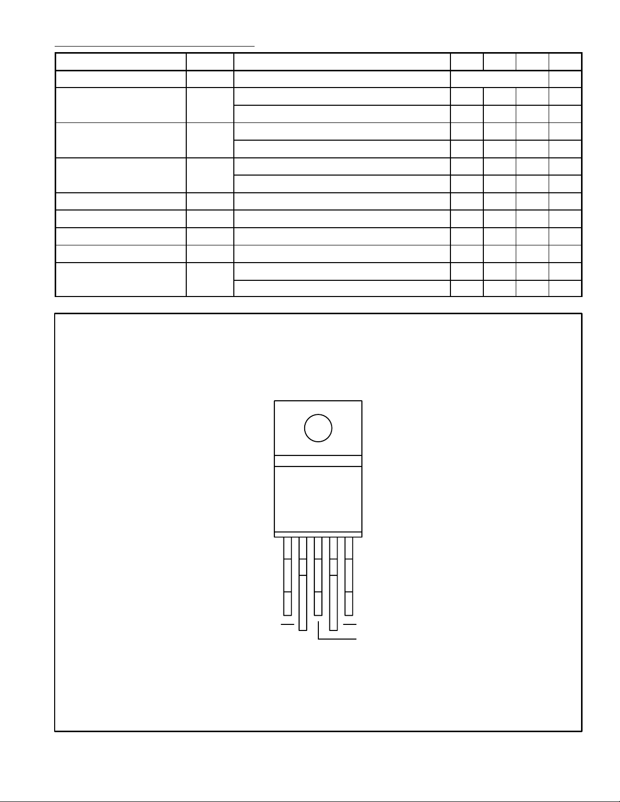
Pin Connection Diagram
(Front View)
Non–Inverting Input (+) V
Inverting Input Output
(–) V
S
/Tab
S
 Loading...