

NTE NTE1367 Datasheet
NTE1367
Integrated Circuit
Dual, Audio Power Amp, 2.3W to 5W
(4.6W to 15W BTL)
Description:
The NTE1367 is an integrated circuit in an 18–Lead DIP type package designed for use in audio output applications with low noise, low distortion and high output widely ranging for power supply and
load resistance. Two amps are built in allowing for dual or BTL operation.
Features:
D High Output Power, Dual or BTL Operation
D Wide Output Power Settuing Range
D Wide Supply Voltage Range
D Incorprated Automatic Operating Point Stabilizer Circuit
D Low Distortion, Low 1/f Noise, and Low Shock Noise
D High Audio Channel Separation
D Incorporated Phase Converter
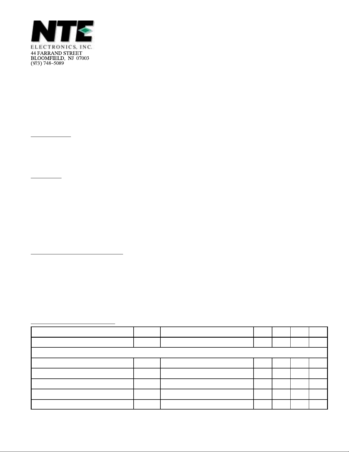
Absolute Maximum Ratings:
Supply Voltage, (Note 1), V
Supply Current, I
Power Dissipation (T
CC
= +60°C), P
A
Operating Ambient temperature Range, T
Storage Temperature Range, T
(TA = +25°C unless otherwise specified)
CC
D
opr
stg
–30° to +75°C. . . . . . . . . . . . . . . . . . . . . . . . . . . . . . . . . .
–55° to +150°C. . . . . . . . . . . . . . . . . . . . . . . . . . . . . . . . . . . . . . . . . .
Note 1. VCC at operation mode = 20V (stabilized power source).
Electrical Characteristics: (TA = +25°C, VCC = 9V, Note 2 unless otherwise specified)
Parameter Symbol Test Conditions Min Typ Max Unit
Quiescent Circuit Current I
BTL (RL = 8Ω, f = 1kHz)
Voltage Gain G
Total Harmonic Distortion THD Vi = 4mV – 0.4 1.0 %
Output Power P
Output Noise Voltage V
Output Offset Voltage V
CQ
O(offset)Vi
Vi = 0 20 32 55 mA
Vi = 4mV 46 48 50 dB
V
THD = 10% 4.3 4.6 – W
O
Vi = 0, Rg = 3.9kΩ – 0.7 1.5 mV
no
= 0 –100 0 +100 mV
20V. . . . . . . . . . . . . . . . . . . . . . . . . . . . . . . . . . . . . . . . . . . . . . . . . . . . . . . .
4A. . . . . . . . . . . . . . . . . . . . . . . . . . . . . . . . . . . . . . . . . . . . . . . . . . . . . . . . . . . . . . . . . .
20W. . . . . . . . . . . . . . . . . . . . . . . . . . . . . . . . . . . . . . . . . . . . . . . . .
Note 2. The value of Typ. is a reference value.
Electrical Characteristics (Cont’d): (TA = +25°C, VCC = 9V, Note 2 unless otherwise specified)
Parameter Symbol Test Conditions Min Typ Max Unit
Dual (RL = 4Ω, f = 1kHz)
Voltage Gain G
Vi = 4mV 42 44 46 dB
V
Total Harmonic Distortion THD Vi = 4mV – 0.3 1.0 %
Output Power P
Output Noise Voltage V
THD = 10% 2.0 2.3 – W
O
Vi = 0, Rg = 3.9kΩ – 0.4 1.0 mV
no
Channel Balance CB Vi = 4mV – 0 1 dB
Note 2. The value of Typ. is a reference value.
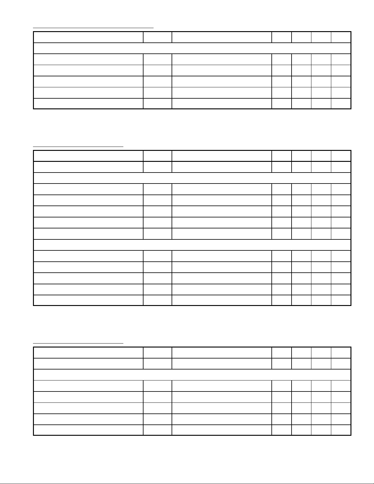
Electrical Characteristics:
Parameter Symbol Test Conditions Min Typ Max Unit
Quiescent Circuit Current I
BTL (RL = 8Ω, f = 1kHz)
Voltage Gain G
Total Harmonic Distortion THD Vi = 4mV – 0.4 1.0 %
Output Power P
Output Noise Voltage V
Output Offset Voltage V
Dual (RL = 4Ω, f = 1kHz)
(TA = +25°C, VCC = 12V, Note 2 unless otherwise specified)
CQ
O(offset)Vi
Vi = 0 20 35 60 mA
Vi = 4mV 46 48 50 dB
V
THD = 10% 7.5 8.3 – W
O
Vi = 0, Rg = 10kΩ – 0.7 2.0 mV
no
= 0 –100 0 +100 mV
Voltage Gain G
Vi = 4mV 42 44 46 dB
V
Total Harmonic Distortion THD Vi = 4mV – 0.3 1.0 %
Output Power P
Output Noise Voltage V
THD = 10% 3.6 4.0 – W
O
Vi = 0, Rg = 3.9kΩ – 0.5 1.5 mV
no
Channel Balance CB Vi = 4mV – 0 1 dB
Note 2. The value of Typ. is a reference value.
Electrical Characteristics:
Parameter Symbol Test Conditions Min Typ Max Unit
Quiescent Circuit Current I
BTL (RL = 8Ω, f = 1kHz)
Voltage Gain G
Total Harmonic Distortion THD Vi = 4mV – 0.4 1.0 %
Output Power P
Output Noise Voltage V
Output Offset Voltage V
(TA = +25°C, VCC = 13.2V, Note 2 unless otherwise specified)
CQ
O(offset)Vi
Vi = 0 20 38 60 mA
Vi = 4mV 46 48 50 dB
V
THD = 10% 9.4 10 – W
O
Vi = 0, Rg = 10kΩ – 0.7 2.0 mV
no
= 0 –100 0 +100 mV
Note 2. The value of Typ. is a reference value.
 Loading...