

NTE NTE133 Datasheet
NTE133
N–Channel JFET Silicon Transistor
General Purpose AF Amplifier
Absolute Maximum Ratings: (TA = +25°C unless otherwise specified)
Drain–Source Voltage, V
Drain–Gate Voltage, V
Gate–Source Voltage, V
Gate Current, I
G
Total Device Dissipation (T
Derate Above 25°C 2mW/°C. . . . . . . . . . . . . . . . . . . . . . . . . . . . . . . . . . . . . . . . . . . . . . . . . . . . . . .
DS
DG
GS
= +25°C), P
A
D
25V. . . . . . . . . . . . . . . . . . . . . . . . . . . . . . . . . . . . . . . . . . . . . . . . . . . . . . . . . .
25V. . . . . . . . . . . . . . . . . . . . . . . . . . . . . . . . . . . . . . . . . . . . . . . . . . . . . . . . . . . .
–25V. . . . . . . . . . . . . . . . . . . . . . . . . . . . . . . . . . . . . . . . . . . . . . . . . . . . . . . . .
10mA. . . . . . . . . . . . . . . . . . . . . . . . . . . . . . . . . . . . . . . . . . . . . . . . . . . . . . . . . . . . . . . . . .
300mW. . . . . . . . . . . . . . . . . . . . . . . . . . . . . . . . . . . . . . . . .
Operating Junction Temperature Range, T
Storage Temperature Range, T
stg
Lead Temperature (During Soldering, 1/16” from case for 10sec), T
Electrical Characteristics:
Parameter Symbol Test Conditions Min Typ Max Unit
Gate–Source Breakdown Voltage V
Gate Reverse Current I
Gate–Source Cutoff Voltage V
Gate–Source Voltage V
Zero–Gate–Voltage Drain Current I
Forward Transfer Admittance |yfs| VDS = 15V, VGS = 0, f = 1kHz 1000 – 7500 µmho
(TA = +25°C unless otherwise specified)
(BR)GSSIG
GSS
GS(off)ID
DSS
GS
J
L
= 1µA, VDS = 0 –25 – – V
VGS = 20V, VDS = 0 – – –1 nA
VGS = 20V, VDS = 0, TA = +150°C – – –1 µA
= 1µA, VDS = 15V – – –6.5 V
ID = 50µA, VDS = 15V –0.4 – –6.0 V
VDS = 15V, VGS = 0 0.5 – 15 mA
–55° to +150°C. . . . . . . . . . . . . . . . . . . . . . . . . . . . . . . . . .
–55° to +150°C. . . . . . . . . . . . . . . . . . . . . . . . . . . . . . . . . . . . . . . . . .
+260°C. . . . . . . . . . . . . . . . . . .
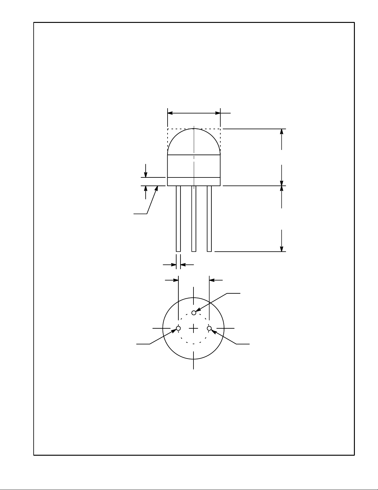
.060
(1.52)
Min
.207 (5.28) Dia
.180
(4.57)
Seating
Plane
Source
.500
(12.7)
Min
.018 (0.45)
.100 (2.54) Dia
Drain
Gate
 Loading...