

NTE NTE1294 Datasheet

NTE1294
Integrated Circuit
Audio Power Amplifier, 1.2W
Description:
The NTE1294 is a monolithic integrated audio amplifier in an 8–Lead DIP type package designed for
use as a low frequency class B power amplifier with a wide supply voltage range (3V to 16V) in portable radios, cassette recorders, and players etc.
Features:
D Minimum Working Supplu Voltage: Vs = 3V Min
D Low Quiescent Current
D Low Number of External Components
D Good Ripple Rejection
D No Cross–over Distortion
D Low Power Dissipation
D Output Power:
Po = 2W at 12V/8Ω
Po = 1.6W at 9V/4Ω
Po = 1.2W at 9V/8Ω
Absolute Maximum Ratings:
Supply Voltage, V
Output Peak Current, I
Power Dissipation (TA = +50°C), P
Junction Temperature Range, T
Storage Temperature Range, T
Maximum Thermal Resistance, Junction–to–Ambient, R
s
o
tot
J
stg
thJA
Electrical Characteristics: (VS = 9V, TA = +25°C unless otherwise specified)
Parameter Symbol Test Conditions Min Typ Max Unit
Supply Voltage V
Quiescent Output Voiltage (Pin5) V
Quiescent Drain Current I
Bias Current (Pin3) I
s
o
d
b
3 – 16 V
4.0 4.5 5.0 V
– 4 12 mA
– 0.1 – µA
16V. . . . . . . . . . . . . . . . . . . . . . . . . . . . . . . . . . . . . . . . . . . . . . . . . . . . . . . . . . . . . . . . .
1.5A. . . . . . . . . . . . . . . . . . . . . . . . . . . . . . . . . . . . . . . . . . . . . . . . . . . . . . . . . . . .
1W. . . . . . . . . . . . . . . . . . . . . . . . . . . . . . . . . . . . . . . . . . . . . . . . . .
–40° to +150°C. . . . . . . . . . . . . . . . . . . . . . . . . . . . . . . . . . . . . . . . . . .
–40° to +150°C. . . . . . . . . . . . . . . . . . . . . . . . . . . . . . . . . . . . . . . . . .
100°C/W. . . . . . . . . . . . . . . . . . . . . . . .
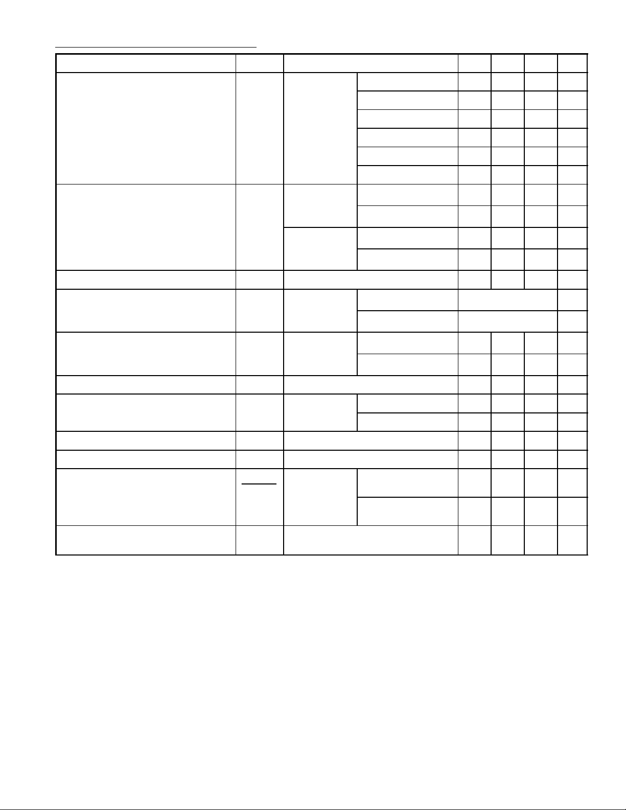
Electrical Characteristics (Cont’d): (VS = 9V, TA = +25°C unless otherwise specified)
R = 120
Ω
Parameter Symbol Test Conditions Min Typ Max Unit
Output Power P
o
d = 10%,
f = 1kHz,
Ω
Input Sensitivity V
i(rms)
Rf = 120
Po = 1.2W,
RL = 8Ω,
f = 1kHz
Po = 50mW,
RL = 8Ω,
f = 1kHz
Input Resistance (Pin3) R
f = 1kHz – 5 – MΩ
i
Frequency Response (–3dB) B RL = 8Ω,
C5 = 1000µF,
R
= 120Ω
f
Distortion d Po = 500mW,
RL = 8Ω,
f = 1kHz
Vs = 12V, RL = 8Ω – 2 – W
Vs = 9V, RL = 4Ω – 1.6 – W
Vs = 9V, RL = 8Ω 0.9 1.2 – W
Vs = 6V, RL = 4Ω – 0.75 – W
Vs = 3.5V, RL = 4Ω – 0.25 – W
Vs = 3V, RL = 4Ω – 0.20 – W
Rf = 33Ω – 16 – mV
Rf = 120Ω – 60 – mV
Rf = 33Ω – 3.5 – mV
Rf = 120Ω – 12 – mV
CB = 680pF 25 to 7000 Hz
CB = 220pF 25 to 20000 Hz
Rf = 33Ω – 0.8 – %
Rf = 120Ω – 0.4 – %
Voltage Gain (Open Loop) G
Voltage Gain (Closed Loop) G
f = 1kHz, RL = 8Ω – 75 – dB
v
RL = 8Ω,
v
f = 1kHz
Input Noise Voltage e
Input Noise Current i
Signal to Noise Ratio
S + N
N
N
Note 1 – 3 – µV
N
Note 1 – 0.4 – nA
N
Po = 1.2W,
R
= 8Ω,
L
L
Gv = 34dB,
Note 1
Supply Voltage Rejection SVR RL = 8Ω, f
C6 = 47µF, R
Note 1. B = 22Hz to 22kHz
Rf = 33Ω – 45 – dB
Rf = 120Ω – 34 – dB
R1 = 10kΩ – 80 – dB
R1 = 50kΩ – 70 – dB
ripple
= 120Ω
f
= 100Hz,
– 42 – dB
 Loading...